Semiconductor structure and forming method thereof

A technology of semiconductor and interconnection structure, which is applied in the direction of semiconductor devices, semiconductor/solid-state device manufacturing, semiconductor/solid-state device components, etc. The effect of increasing the value, reducing the difficulty, and simplifying the process

Inactive Publication Date: 2017-12-05
HUAIAN IMAGING DEVICE MFGR CORP
View PDF3 Cites 2 Cited by
  • Summary
  • Abstract
  • Description
  • Claims
  • Application Information

AI Technical Summary

Problems solved by technology

[0004] However, in the back-end process, although the capacitor (MIM capacitor) required by the integrated circuit can be fabricated in the low-K dielectric layer, the capacitance value per unit area is too small due to the influence of the low dielectric constant of the low-K material. As a result, the overall area of ​​the entire capacitor is larger, which reduces the integration of the circuit

Method used


Image

  • Semiconductor structure and forming method thereof
  • Semiconductor structure and forming method thereof
  • Semiconductor structure and forming method thereof

Examples


Embodiment Construction

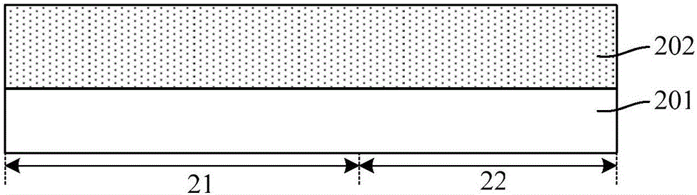
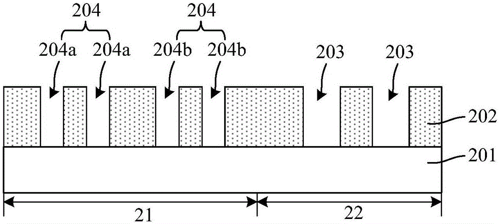
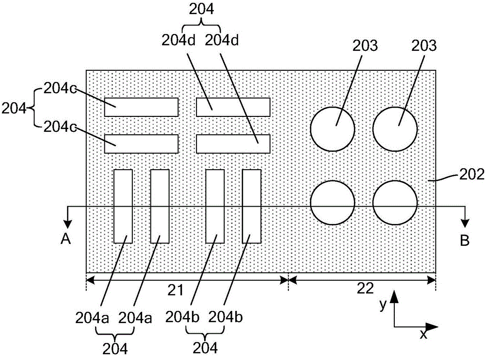
[0027] As mentioned in the background, in the prior art, when a capacitor is formed in a low-K dielectric layer, the overall area of ​​the capacitor is relatively large, which reduces the degree of integration of the circuit.

[0028] In order to solve the above problems, the present invention provides a semiconductor structure and a method for forming the same. In the method of the present invention, the area occupied by the capacitor formed in the low-K dielectric layer is small, and the integration of the capacitor and the interconnection structure (plug) is realized. make.

[0029] In order to make the above objects, features and advantages of the present invention more comprehensible, specific embodiments of the present invention will be described in detail below in conjunction with the accompanying drawings. When describing the embodiments of the present invention in detail, for convenience of explanation, the schematic diagrams will not be partially enlarged according t...


PUM


Abstract

The invention discloses a semiconductor structure and a forming method thereof, and the method comprises the steps: providing a substrate which comprises a first region and a second region; forming a low-K dielectric layer on the surface of the substrate; carrying out the etching of the low-K dielectric layers in the first and second regions, forming a plurality of openings at the low-K dielectric layer in the first region, and forming a plurality of grooves at the low-K dielectric layer of the second region; placing metal in the first openings and the grooves, forming two opposite plate electrodes of a plurality of capacitors at the low-K dielectric layer in the first region, and forming a plurality of interconnection structures at the low-K dielectric layer of the second region; removing the low-K dielectric layer between the two opposite plate electrodes in the first region, and forming a second opening between the two opposite plate electrodes; placing a high-K dielectric layer in the second opening, wherein the high-K dielectric layer serves as the dielectric material layer of a capacitor. The method achieves the integrated manufacturing of capacitors and interconnection structures in the low-K dielectric layers, and reduces the area of the capacitors.

Description

technical field [0001] The invention relates to the field of semiconductor manufacturing, in particular to a semiconductor structure and a forming method thereof. Background technique [0002] With the continuous development of semiconductor integrated circuit technology, the size of semiconductor devices and the size of interconnection structures are continuously reduced, resulting in the gradual reduction of the spacing between metal wirings, and the dielectric layer used to isolate metal wirings is becoming more and more Thinner and thinner, this will cause crosstalk between metal connections. Reducing the dielectric constant K of the dielectric layer can solve the crosstalk problem, and can also effectively reduce the resistance-capacitance (RC) delay of the interconnection. Therefore, in deep submicron technology, low-K materials and ultra-low-K materials have been increasingly used in back-end interconnection processes. [0003] Capacitive components are often used a...

Claims


Application Information

Patent Timeline
Patent Type & Authority Applications(China)
IPC IPC(8): H01L21/768H01L23/522
CPCH01L21/76801H01L21/76837H01L23/5223H01L28/40
Inventor 柯天麒尹扬姜鹏
Owner HUAIAN IMAGING DEVICE MFGR CORP
Why Eureka
Try Eureka