OLED substrate and manufacturing method and display apparatus
A manufacturing method and substrate technology, applied in semiconductor/solid-state device manufacturing, electrical components, electrical solid-state devices, etc., can solve problems such as easy disconnection of electrode leads, and achieve reliable molding, simple and reliable process, and reliable connection.
- Summary
- Abstract
- Description
- Claims
- Application Information
AI Technical Summary
Problems solved by technology
Method used
Image

Examples
Embodiment 1
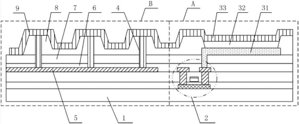
[0064] see figure 2, in the OLED substrate provided in Embodiment 1, the active layer 21 of the thin film transistor is arranged on the base substrate 1, and the gate insulating layer 10 is arranged on the active layer 21, and the gate insulating layer 10 corresponds to the surface of the active layer 21 A gate 22 is provided, and the gate insulating layer 10 is located on the surface of the peripheral wiring area B, and a signal line 5 on the same layer as the gate 22 is provided; the gate 22, the gate insulating layer 10 and the signal line 5 are all covered with an interlayer insulating layer 11, and part of the signal line 5 is covered by the interlayer insulating layer 11, partly exposed outside the edge of the interlayer insulating layer 11; the surface of the interlayer insulating layer 11 corresponding to the active layer 21 is provided with a source and drain 23, and the source and drain 23 includes a source electrode and a drain electrode, and the source electrode a...
Embodiment 2
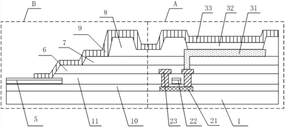
[0072] see image 3 , in the OLED substrate provided in the second embodiment, the structure of the thin film transistor, the structure of the OLED, the position of the signal line 5 and the arrangement of the functional film layer between the signal line 5 and the OLED cathode 33 are all the same as those of the first embodiment.
[0073] In the OLED substrate provided in this embodiment, the electrode leads include a first segment of sub-segment leads 91 connected to the portion of the signal line 5 not covered by the interlayer insulating layer 11, and a first segment of sub-segment leads 91 overlapping with the first segment of sub-segment leads 91. Two segments of sub-segment leads 92, and the second segment of sub-segment leads 92 are connected to the cathode 33 of the OLED.
[0074] Specifically, the first segment of sub-segment lead 91 is correspondingly arranged on the edge surface of the interlayer insulating layer 11, and the first segment of sub-segment lead 91 and...
Embodiment 3
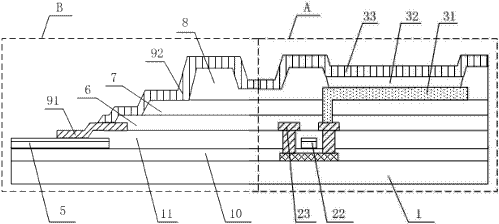
[0076] see Figure 4 , in the OLED substrate provided in the third embodiment, the structure of the thin film transistor, the structure of the OLED, the position of the signal line 5 and the functional film layer between the signal line 5 and the OLED cathode 33 are all the same as the first embodiment.
[0077] In the OLED substrate provided in this embodiment, the electrode leads include a first subsection lead 91 connected to the part of the signal line 5 not covered by the interlayer insulating layer 11, and a second subsection lead 91 overlapping the first section subsection lead 91. A sub-segment lead 92, and a third sub-segment lead 93 overlapped with the second sub-segment lead 92, and the third sub-segment lead 93 is connected to the cathode 33 of the OLED.
[0078] Specifically, the first segment of sub-segment lead 91 is correspondingly arranged on the edge surface of the interlayer insulating layer 11, and the first segment of sub-segment lead 91 and the source and...
PUM
 Abstract
Description
Claims
Application Information
 - R&D
- Intellectual Property
- Life Sciences
- Materials
- Tech Scout
- Unparalleled Data Quality
- Higher Quality Content
- 60% Fewer Hallucinations
Browse by: Latest US Patents, China's latest patents, Technical Efficacy Thesaurus, Application Domain, Technology Topic, Popular Technical Reports.
© 2025 PatSnap. All rights reserved.Legal|Privacy policy|Modern Slavery Act Transparency Statement|Sitemap|About US| Contact US: help@patsnap.com