Large-size light emitting diode epitaxial wafer and growing method thereof

A technology for light emitting diodes and a growth method, which is applied in the production of light emitting diode epitaxial structures and in the field of semiconductors, can solve the problems of poor uniformity of epitaxial slivers and epitaxial wafers, and achieve the effects of improving wavelength uniformity, improving quality, and solving process difficulties.

Inactive Publication Date: 2017-12-08
YANGZHOU ZHONGKE SEMICON LIGHTING
View PDF2 Cites 7 Cited by
  • Summary
  • Abstract
  • Description
  • Claims
  • Application Information

AI Technical Summary

Problems solved by technology

[0004] Aiming at the problems of growing epitaxial splits and poor uniformity of epitaxial wafers on large-sized substrates, the present invention proposes a large-sized light-emitting diode epitaxial wafer and a growth method thereof

Method used


Image

  • Large-size light emitting diode epitaxial wafer and growing method thereof
  • Large-size light emitting diode epitaxial wafer and growing method thereof

Examples


Embodiment Construction

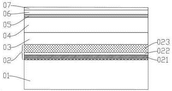
[0021] 1. Production process:

[0022] The epitaxial structure of the present invention is grown by MOCVD, H 2 , N 2 Carrier gas as organometallic source, SiH 4 Provides N-type doping, magnesiumocene (Cp 2 Mg) provides P-type doping, NH 3 As group V source, trimethylgallium (TMGa), triethylgallium (TEGa), trimethylaluminum (TMAl), trimethylindium (TMIn), as group III organometallic source.

[0023] Such as figure 1 As shown, the growth steps are as follows:

[0024] Step 1: Raise the temperature of the MOCVD reaction chamber to 250°C and feed NH 3 and trimethylindium (TMIn), grow InN with a thickness of 100nm on the substrate 01 as the first buffer layer 021, and the growth pressure is 300mbar.

[0025] The substrate 01 can be selected from sapphire, Si, SiC, GaN, etc. In this example, a 6-inch sapphire substrate is preferred.

[0026] Step 2: In H 2 Under ambient conditions, raise the temperature of the MOCVD reaction chamber to 1200°C to perform a high-temperature c...


PUM


Abstract

The invention discloses a large-size light emitting diode epitaxial wafer and a growing method thereof, and belongs to the technical field of semiconductors. A substrate is provided with a buffer layer, an unintentional doped GaN layer, an N-type doped GaN layer, a multiple quantum well layer, an electronic blocking layer and a P-type doped GaN layer which successfully and epitaxially grows on the substrate, wherein the buffer layer growth includes the successful growth of a first, a second and a third buffer layer on the substrate. According to the invention, three buffer layers are employed to effectively release the stress which is generated due to the differences of coefficients of thermal expansion between the substrate and the GaN, to reduce the stress which is generated due to the differences of lattice constants between the substrate and the GaN, to reduce the probability of tattering and shredding of the substrate when the large-size epitaxial wafer grows at high temperature, provides sound basis for the growth of the unintentional doped GaN layer and active layer structure in a nitride thin film structure layer. The substrate herein can increase the quality of large-size epitaxial material, improve the uniformity of the wavelength of the epitaxial wafer and adjusts the warpage of the epitaxial wafer.

Description

technical field [0001] The invention belongs to the technical field of semiconductors, and in particular relates to the technical field of production of light-emitting diode epitaxial structures. technical background [0002] In recent years, nitride-based LED chips have been widely used in many fields such as display screens, backlights, lighting, and street lamps. With the large-scale application of LEDs, the market has put forward higher requirements for LED production efficiency and production costs. Epitaxy To continue to reduce LED manufacturing costs, the use of larger substrates has become an inevitable trend. [0003] At present, the epitaxial wafers in the LED market are mainly 4 inches and 2 inches. The epitaxial technology of 6 inches or even larger is not yet mature. One of the main reasons is that large-sized epitaxial wafers are prone to cracks and fragments during the growth process. , and the uniformity of the epitaxial wafer is poor, and the product yield ...

Claims


Application Information

Patent Timeline
Patent Type & Authority Applications(China)
IPC IPC(8): H01L33/12H01L33/00
CPCH01L33/12H01L33/007
Inventor 张韧剑李志聪冯亚萍王国宏
Owner YANGZHOU ZHONGKE SEMICON LIGHTING
Why Eureka
Try Eureka