A filter circuit and chip based on mos field effect transistor

A field effect transistor and filter circuit technology, applied in the field of filter circuits and chips, can solve the problems of not having ESD and threatening the safety of internal devices of the chip, and achieve the effect of filtering out AC interference and enhancing ESD capability.

Active Publication Date: 2021-03-16
SHENZHEN GOODIX TECH CO LTD
View PDF3 Cites 0 Cited by
  • Summary
  • Abstract
  • Description
  • Claims
  • Application Information

AI Technical Summary

Problems solved by technology

This kind of filter circuit generally only has capacitance characteristics, and does not have ESD (Electro-Static discharge, electrostatic discharge) characteristics. How...

Method used


Image

  • A filter circuit and chip based on mos field effect transistor
  • A filter circuit and chip based on mos field effect transistor
  • A filter circuit and chip based on mos field effect transistor

Examples


Embodiment Construction

[0025] In order to make the purpose, technical solution and advantages of the present application clearer, some embodiments of the present application will be further described in detail below in conjunction with the accompanying drawings and embodiments. It should be understood that the specific embodiments described here are only used to explain the present application, and are not intended to limit the present application.

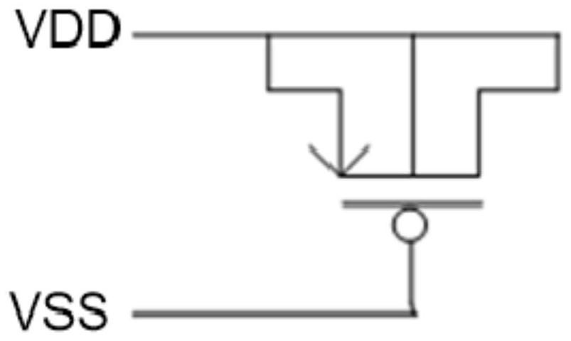
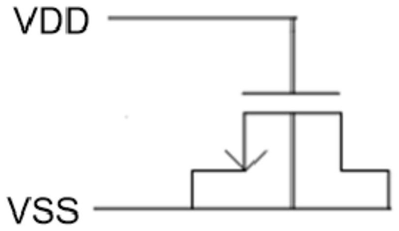
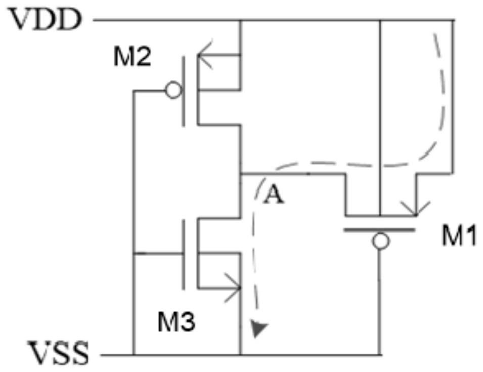
[0026] The first embodiment of the present application relates to a filter circuit based on MOS field effect transistors. The filter circuit includes a first MOS field effect transistor and an electrostatic discharge unit.

[0027] The electrostatic discharge unit can be composed of a plurality of MOS field effect transistors, and cooperate with the first MOS field effect transistor, so that in normal operation, a MOS capacitor can be formed between the gate and the substrate of the first MOS field effect transistor as The filter capacitor makes the fi...


PUM


Abstract

Some embodiments of the present application provide a filter circuit and chip based on MOS field effect transistors. The filter circuit includes a first MOS field effect transistor and an electrostatic discharge unit; during normal operation, a filter capacitor is formed between the gate of the first MOS field effect transistor and the substrate; when an ESD event occurs, the electrostatic discharge unit and the first A MOS field effect transistor forms a discharge path that transfers the accumulated electrostatic charge to ground. In the embodiment of the present application, on the basis of the first MOS field effect transistor, an electrostatic discharge unit is added, so that the capacitance characteristics and the characteristics of the ESD discharge path required between the power supply and the ground are combined in the same circuit, so that the circuit can be used in the same circuit. It exhibits capacitive characteristics during normal operation; when an ESD event occurs between the power supply and ground, it provides an ESD discharge path to play the role of ESD protection, thereby improving the ESD capability of the chip.

Description

technical field [0001] The present application relates to the technical field of integrated circuits, in particular to a filter circuit and chip based on MOS field effect transistors. Background technique [0002] In the final stage of chip design, a filter circuit from power supply to ground is generally added to the spare part of the chip. The selected filter capacitor can be MOS (Metal-Oxide-Semiconductor, metal-oxide-semiconductor) field effect transistor capacitor, MIM (Metal-Insulator-Metal, metal-insulator-metal) capacitor, MOM (Metal-Oxide-Metal, metal-oxide-metal) capacitors, etc. However, considering that the capacitance per unit area of ​​MOS field effect transistor capacitors (hereinafter referred to as MOS capacitors) is larger than that of other capacitors, a larger capacitor can be obtained under the same area. Therefore, under normal circumstances, MOS capacitors are usually selected as filter capacitor. [0003] MOS capacitors are divided into two types: ...

Claims


Application Information

Patent Timeline
IPC IPC(8): H01L27/02H03H11/38
CPCH01L27/0266H01L27/0296H03H11/38H01L27/027H01L27/0274H01L27/0285H02H9/046
Inventor 陈建兴
Owner SHENZHEN GOODIX TECH CO LTD
Why Eureka
Try Eureka