Bit structure of multi-state magnetic memory
A magnetic memory and magnetic tunnel junction technology, which is applied in the field of non-volatile memory and semiconductor, can solve the problems that the size of the triode cannot be made too small and the storage density of magnetic memory is limited, so as to achieve fast reading speed and improve data storage. Density, energy consumption and radiation resistance
- Summary
- Abstract
- Description
- Claims
- Application Information
AI Technical Summary
Problems solved by technology
Method used
Image
Examples
Embodiment 1
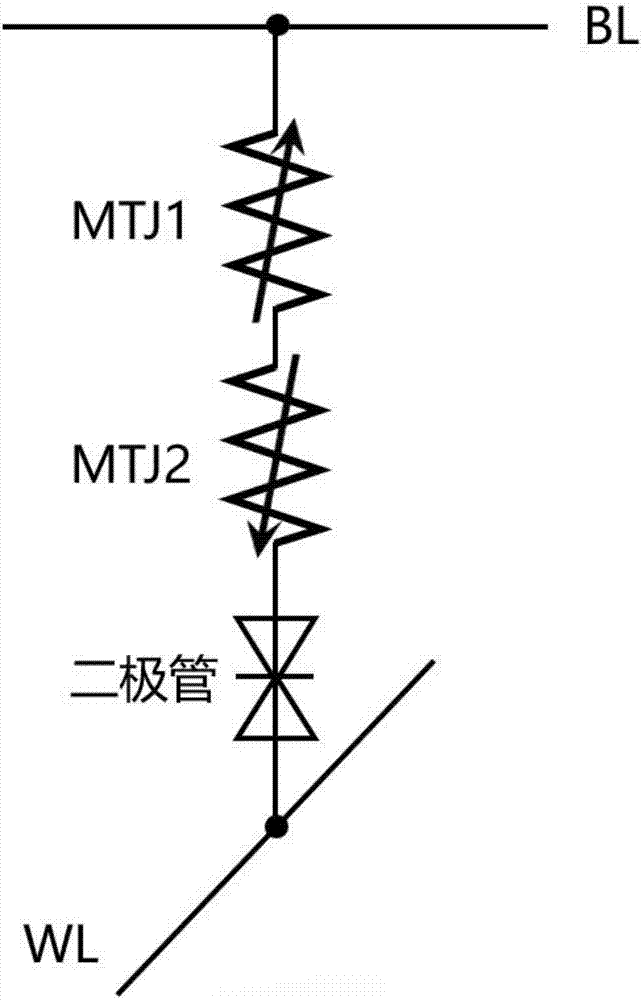
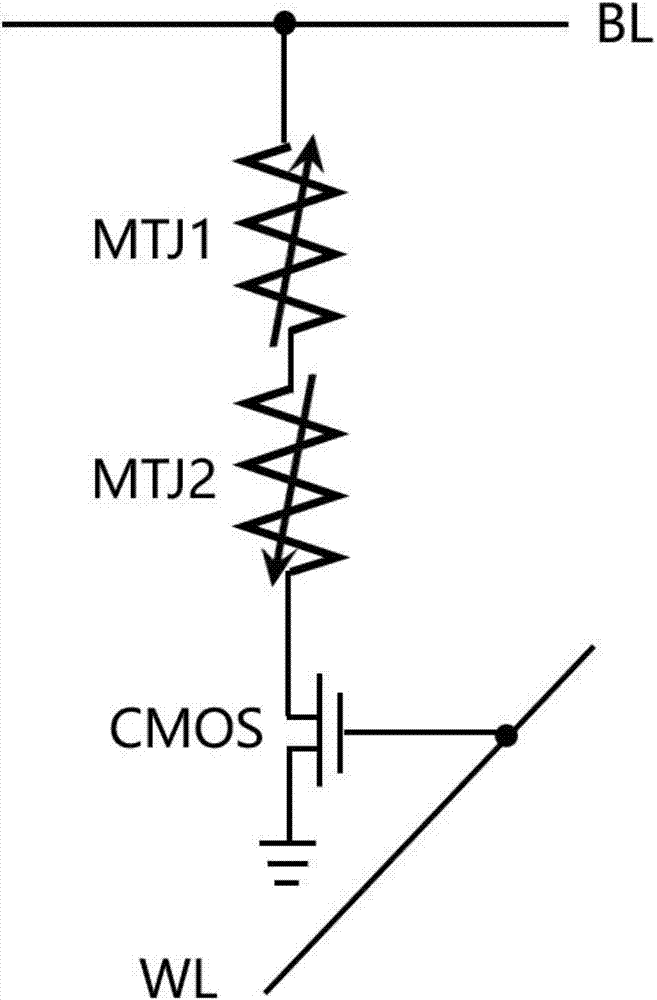
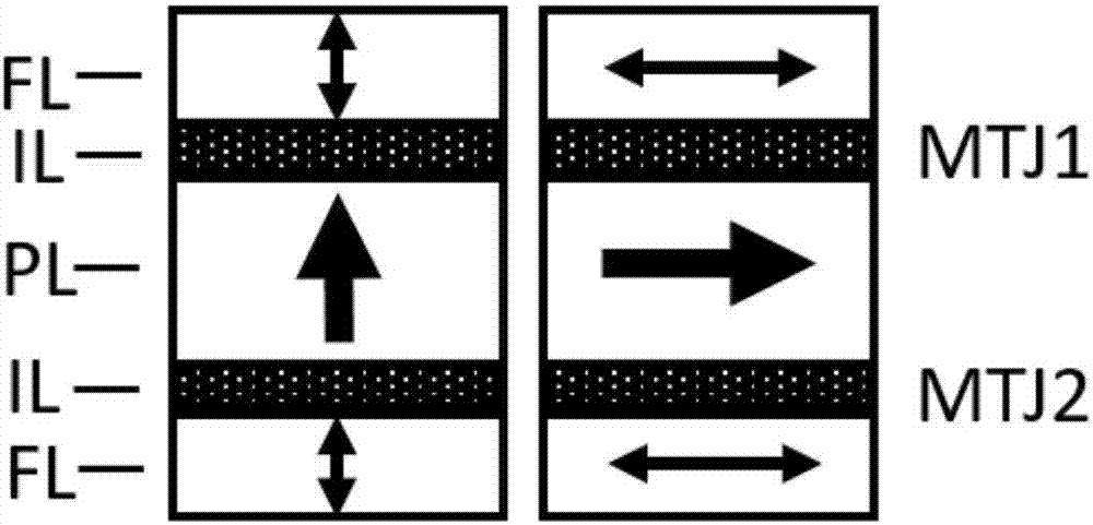
[0023] Example 1: figure 1 The reference signs are: word line WL, bit line BL, magnetic tunnel junction MTJ, and the switch is a diode; figure 2 The reference signs are: word line WL, bit line BL, magnetic tunnel junction MTJ, and the switch is a CMOS transistor; Figure 3 to Figure 6 Reference numerals are: free magnetic layer FL (Free Layer), pinned magnetic layer PL (Pinned Layer), insulating layer IL (Insulating Layer), magnetic tunnel junction MTJ.
[0024] In this embodiment, the bit structure of the multi-state magnetic memory is as follows figure 1 As shown, it includes a multi-state magnetic memory cell composed of a word line WL, a bit line BL, a magnetic tunnel junction 1MTJ1 and a magnetic tunnel junction 2MTJ2, and a memory cell selection switch composed of a diode. Memory cell selection switches can also use CMOS transistors, such as figure 2 shown. One of the above two structures can be selected.
[0025] Wherein, the magnetization of the magnetic layer...
Embodiment 2
[0027] Embodiment 2: In this embodiment, the bit structure of the multi-state magnetic memory is as figure 1 As shown, it includes a multi-state magnetic memory cell composed of a word line WL, a bit line BL, a magnetic tunnel junction 1MTJ1 and a magnetic tunnel junction 2MTJ2, and a memory cell selection switch composed of a diode. Memory cell selection switches can also use CMOS transistors, such as figure 2 shown. One of the above two structures can be selected.
[0028] Wherein, the magnetization of the magnetic layers of MTJ1 and MTJ2 is magnetized horizontally or vertically along the in-plane direction, and the positions of the pinned layers of MTJ1 and MTJ2 are different, one pinned layer is at the bottom, and the other pinned layer is at the top. The pinning directions of the pinned layers of MTJ1 and MTJ2 are the same.
[0029] In this embodiment, the multi-state magnetic tunnel junction memory cell such as Figure 4 As shown, two MTJs are interconnected by wire...
Embodiment 3
[0030] Embodiment 3: In this embodiment, the bit structure of the multi-state magnetic memory is as figure 1 As shown, it includes a multi-state magnetic memory cell composed of a word line WL, a bit line BL, a magnetic tunnel junction 1MTJ1 and a magnetic tunnel junction 2MTJ2, and a memory cell selection switch composed of a diode. Memory cell selection switches can also use CMOS transistors, such as figure 2 shown. One of the above two structures can be selected.
[0031] Wherein, the magnetization of the magnetic layers of MTJ1 and MTJ2 is magnetized horizontally or vertically along the in-plane direction, and the positions of the pinned layers of MTJ1 and MTJ2 are different, one pinned layer is at the bottom, and the other pinned layer is at the top. The pinning directions of the pinned layers of MTJ1 and MTJ2 are the same.
[0032] In this embodiment, the multi-state magnetic tunnel junction memory cell such as Figure 5 As shown, two MTJs are interconnected by wire...
PUM
 Abstract
Description
Claims
Application Information


