[0035] In order to make the objectives, technical solutions, and advantages of the present disclosure clearer, the following further describes the present disclosure in detail with reference to specific embodiments and drawings.
[0036] It should be noted that in the drawings or description of the specification, similar or identical parts use the same drawing numbers. The implementations not shown or described in the drawings are those known to those of ordinary skill in the art. In addition, although this article may provide an example of a parameter containing a specific value, it should be understood that the parameter does not need to be exactly equal to the corresponding value, but can be approximated to the corresponding value within acceptable error tolerances or design constraints. The directional terms mentioned in the embodiments, such as "upper", "lower", "front", "rear", "left", "right", etc., are only directions with reference to the drawings. Therefore, the directional terms used are used to illustrate and not to limit the protection scope of the present disclosure.
[0037] The present disclosure provides an AlN substrate high-efficiency heat dissipation HEMT device and a preparation method thereof. The high-efficiency heat dissipation HEMT device of the AlN substrate of the present disclosure and a preparation method thereof will be described in detail below with reference to the accompanying drawings.
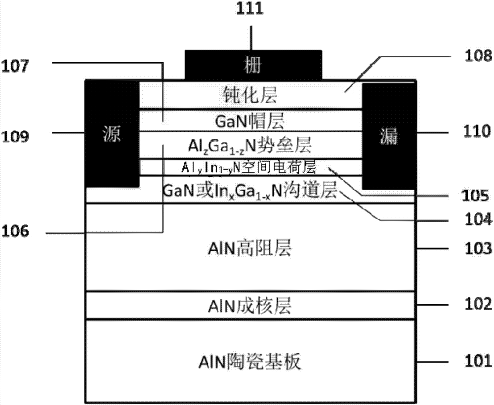
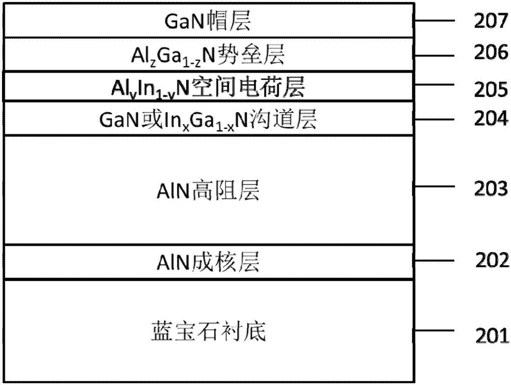
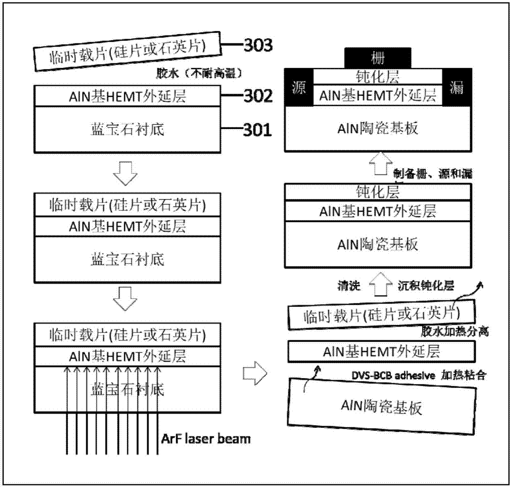
[0038] 1. HEMT device structure for efficient heat dissipation of AlN substrate
[0039] figure 1 It is a schematic diagram of the structure of the HEMT device with high efficiency heat dissipation on the Al substrate of the present disclosure. Such as figure 1 As shown, the Al substrate heat dissipation HEMT device includes an AlN ceramic substrate 101, an AlN nucleation layer 102, an AlN high resistance layer 103, GaN or In x Ga 1-x N channel layer 104, Al y In 1-y N space charge layer 105, Al z Ga 1-z N barrier layer 106, GaN cap layer 107, passivation layer 108, source electrode 109, drain electrode 110, and gate electrode 111.
[0040] Compared with the conventional HEMT device structure, the HEMT device structure in the present disclosure uses a high-resistance AlN layer instead of the traditional high-resistance doped GaN layer, which has better insulation and thermal conductivity than the GaN layer, and can effectively reduce parasitic capacitance. The AlInN layer is used to replace the traditional AlGaN or AlN space charge layer, and perfect in-plane lattice matching can be achieved by adjusting the Al or In composition and the GaN or InGaN channel layer, reducing the formation of misfit dislocations in the heterojunction, thereby Reduce the adverse effect of dislocation scattering on the mobility of the two-dimensional electron gas in the channel layer, and improve the performance of the HEMT device. In addition, an AlN ceramic substrate is used to replace the traditional sapphire substrate or silicon substrate.
[0041] The high-efficiency heat dissipation HEMT device of the AlN substrate of the present disclosure improves the performance and heat dissipation capacity of the HEMT device and reduces the preparation cost of the HEMT device.
[0042] 2. Preparation method of AlN substrate for efficient heat dissipation HEMT device
[0043] The preparation method of the high-efficiency heat dissipation HEMT device provided by the present disclosure mainly includes the following steps:
[0044] S1, epitaxial growth of HEMT device structure layer on MOCVD system, please refer to figure 2 As shown, it includes the following sub-steps:
[0045] S11. Put the c-plane or m-plane oriented sapphire substrate into the MOCVD reaction chamber, in H 2 High temperature treatment in the atmosphere.
[0046] S12, in H 2 After cooling the substrate to 600-850°C in an atmosphere, a low-temperature AlN nucleation layer is grown on the substrate with a thickness of 20-60 nm.
[0047] S13, in H 2 Raise the temperature to 1050~1300℃ in the atmosphere, and use the pulse method to grow a high temperature AlN layer with a thickness of 1~5μm;
[0048] S14, in H 2 The GaN channel layer is grown at a high temperature (1020~1100℃) in an atmosphere with a thickness of 20~100nm, or at N 2 Grow In at medium temperature (700~850℃) in atmosphere x Ga 1-x N, the component x is controlled between 0.05 and 0.2, and the thickness is 20 to 100 nm.
[0049] S15, in N 2 Growth of Al at medium temperature (700~850℃) in atmosphere y In 1-y N space charge layer, thickness 1~5nm, adjust composition y to make Al y In 1-y The in-plane lattice constant of the N layer is perfectly matched with the channel layer. For the GaN channel layer, the composition y is controlled at 0.82. For In x Ga 1-x For the N channel layer, because the In composition x is controlled between 0.05 and 0.2, accordingly, the Al composition y is controlled between 0.94 and 0.76.
[0050] S16, in H 2 The AlGaN barrier layer is grown at a high temperature (1020~1080°C) in an atmosphere with a thickness of 20~50nm.
[0051] S17, in H 2 The GaN cap layer is grown at a high temperature (1060-1100°C) in an atmosphere with a growth thickness of 2-5nm.
[0052] S2, peel and transfer the sapphire substrate of the epitaxial layer of HEMT device, please refer to image 3 As shown, it includes the following sub-steps:
[0053] S21. First bonding: Spin-coating ethyl cyanoacrylate as the bonding material on the front surface of the temporary carrier (Si substrate or quartz wafer, etc.) and attach it to the epitaxial layer of the HEMT device, and heat the temporary carrier Bake at 70~90℃, and then bond the temporary slide at room temperature; the bonding agent can also be a bonding agent that can be bonded at room temperature but melts at 100~200℃.
[0054] S22. First peeling: Using laser peeling technology, ArF laser is used to irradiate the side of the sapphire substrate, and the laser focus acts on the interface between the sapphire substrate and the AlN nucleation layer. The laser power and the action time are adjusted to promote the sapphire substrate and The HEMT epitaxial layer is separated, and the separated HEMT device layer is cleaned.
[0055] S23. Second bonding: Spin-coating DVS-BCB on the AlN ceramic substrate as the bonding material, and attach it to the surface of the temporary carrier that contains the epitaxial layer. Place it in a low vacuum environment and heat it to 400 to 500°C. Pre-curing treatment, and then low-temperature annealing to about 100 ~ 200 ℃ for bonding.
[0056] S24. Second peeling: The ethyl cyanoacrylate (or other bonding agent) between the temporary carrier and the epitaxial layer will fall off due to high temperature denaturation, and the HEMT device layer bonded with the AlN substrate will be chemically cleaned.
[0057] S3. Prepare passivation layer, source, gate and drain on HEMT device, please refer to further image 3 As shown, it includes the following sub-steps:
[0058] S31. Use atomic layer epitaxy or plasma enhanced chemical vapor deposition (PECVD) to evaporate a passivation layer (insulating dielectric film) on the HEMT device layer, with a thickness of 0.1-5 microns, and the passivation layer can be Si 3 N 4 , Or Al 2 O 3 , Or ZrO 2 , Or HfO 2 Etc., the passivation layer is treated with fluoride ion to improve device characteristics.
[0059] S32. Coat photoresist on the HEMT device layer, realize the device pattern transfer by soft baking, photolithography exposure, development and other photolithography processes, and etch it to GaN or In by plasma etching x Ga 1-x After the middle position of the N-channel layer, a mesa pattern is obtained to facilitate the preparation of the source and drain of the HEMT in the subsequent process.
[0060] S33: Prepare source and drain electrodes with ohmic contact characteristics on the channel layer mesa through device processes such as photoresist coating, photolithography, exposure, development, vapor deposition of metal materials, alloying annealing and the like.
[0061] S34. Similar to the device process of step S33, a gate electrode with Schottky contact characteristics is prepared by evaporating a metal material on the passivation layer.
[0062] The above-mentioned AlN substrate high-efficiency heat-dissipating HEMT device and its preparation method provided in the present disclosure can be used to manufacture high-power electronic power devices, and are widely used in transportation (automobiles, electric locomotives), communications (base stations), energy (grid power switches), military (Radar) and other fields.
[0063] The epitaxial structure and preparation method of the AlN substrate for efficient heat dissipation HEMT devices provided by the present disclosure can improve the heat dissipation capacity and performance of the HEMT devices, and effectively reduce the cost.
[0064] The following describes in detail the preparation examples of the highly efficient heat dissipation HEMT device of the present disclosure.
[0065] Step 1: Put the c-plane or m-plane oriented sapphire substrate into the MOCVD reaction chamber, and treat it at a high temperature of 1000-1150°C for 2-10 minutes in an H2 atmosphere. The nitride epitaxial layer prepared by selecting (0001) c-plane orientation sapphire substrate has (0001) polar c-plane orientation. Using (1-100) m-plane oriented sapphire substrate can prepare (11-22) plane or (10-1-3) semi-polar plane orientation.
[0066] Step 2: In H 2 After cooling the substrate to 600-850°C in an atmosphere, a low-temperature AlN nucleation layer (thickness 20-60nm) is grown on the substrate, the growth time is 5-10min, and the growth pressure is 20-500 Torr.
[0067] Step 3: In H 2 The temperature is raised to 1050-1300°C in an atmosphere, and a high-temperature AlN layer is grown using a pulse method with a thickness of 1 to 5 μm and a growth pressure of 50-500 Torr.
[0068] Step 4: In H 2 Grow a GaN channel layer at a high temperature (1020~1100℃) in an atmosphere with a thickness of 20~100nm, a growth rate of 0.5-2μm/h, and a growth pressure of 100~500 Torr; or a medium temperature (700~850℃) in a N2 atmosphere Growth In x Ga 1-x N, the composition x is controlled between 0.05 and 0.2, the thickness is 20 to 100 nm, and the growth pressure is 100 to 500 Torr.
[0069] Step 5: In N 2 Growth of Al at medium temperature (700-850℃) in atmosphere y In 1-y The N space charge layer has a thickness of 1 to 5 nm and a growth pressure of 20 to 200 Torr. Adjust component y so that Al y In 1-y The in-plane lattice constant of the N layer is perfectly matched with the channel layer. For the GaN channel layer, according to Vegard’s law, Al y In 1-y The composition y of the N-space layer that is lattice-matched with the channel layer GaN in the growth crystal plane is 0.82. For In x Ga 1-x N-channel layer, according to Vegard’s law, because In x Ga 1-x N, In composition x is controlled between 0.05~0.2, Al y In 1-y The N space layer and the channel layer In x Ga 1-x Composition of N Al y In 1-y The N space charge layer interacts with the In x Ga 1-x The lattice matching composition y of the N-channel layer is controlled between 0.94 and 0.76.
[0070] Step 6: In H 2 The AlGaN barrier layer is grown in an atmosphere with a growth thickness of 20-50nm, a growth rate of 0.1-0.3μm/h, a growth temperature of 1020-1080°C, and a growth pressure of 20-200 Torr. It can be n-type doped appropriately, To reduce the sheet resistance of the device.
[0071] Step 7: In H 2 An unintentionally doped GaN cap layer is grown in an atmosphere with a thickness of 2-5nm, a growth rate of 0.5-2μm/h, a growth temperature of 1060-1100°C, and a growth pressure of 50-500 Torr.
[0072] Step 8: Wash the grown epitaxial wafer and temporary slide (Si wafer or quartz wafer) with dilute hydrochloric acid, then rinse with deionized water and use N 2 Blow dry.
[0073] Step 9: Spin-coat ethyl cyanoacrylate as a bonding material on the front surface of the temporary slide and attach it to the epitaxial layer of the HEMT device, heat the temporary slide to 70~90℃ for baking, and then wait for the temporary slide Bonding at room temperature; the bonding agent can also be paraffin wax, which can bond at room temperature.
[0074] Step 10: Using laser lift-off technology, irradiate the back side of the sapphire substrate with an ArF laser, and the laser focus acts on the interface between the sapphire substrate and the AlN nucleation layer. Adjust the laser power and action time to promote the sapphire substrate and the HEMT epitaxial layer Separate and chemically clean the separated HEMT device layer.
[0075] Step 11: Spin-coating DVS-BCB on the AlN ceramic substrate as a bonding material, attach it to the surface of the temporary carrier containing the epitaxial layer, place it in a low vacuum environment, heat it to 400 to 500°C for pre-curing, and then Low-temperature annealing to about 100-200°C for bonding. The ethyl cyanoacrylate (or other bonding agent) between the temporary carrier sheet and the epitaxial layer will fall off due to high temperature denaturation.
[0076] Step 12: Coating photoresist on the HEMT device layer, after soft baking, photolithography exposure, dry etching (ICP), cleaning and other steps to obtain gate, source and drain mesa, where the source and drain The pole mesa is located in GaN or In x Ga 1-x The middle of the N-channel layer.
[0077] Step 13: Use atomic layer epitaxy or plasma-enhanced chemical vapor deposition (PECVD) to evaporate the passivation layer isolation layer, that is, the insulating dielectric film, with a thickness of 0.1-5 microns, and the passivation layer can be Si 3 N 4 , Or Al 2 O 3 , Or ZrO 2 , Or HfO 2 Etc., the passivation layer is treated with fluoride ion to improve device characteristics.
[0078] Step 14: Prepare source and drain electrodes with ohmic contact characteristics on the channel layer mesa through photoresist coating, photolithography, exposure, development, vapor deposition of source and drain metals, alloying annealing and other device processes pole.
[0079] In step 15, similar to the device process of step 14, the gate metal is evaporated and alloyed on the passivation layer to prepare a gate electrode with Schottky contact characteristics.
[0080] The present disclosure can complete the substrate transfer at one time through the combined use of ethyl cyanoacrylate and the DVS-BCB bonding agent.
[0081] In addition, the process and process parameters, such as temperature, rate, pressure, time, and growth mode in the present disclosure are not limited to those in the embodiments, and those skilled in the art can make appropriate adjustments without affecting the implementation of the present disclosure.
[0082] The above description of the disclosed embodiments enables those skilled in the art to implement or use this application. Various modifications to these embodiments will be obvious to those skilled in the art, and the general principles defined in this document can be implemented in other embodiments without departing from the spirit or scope of the application. Therefore, this application will not be limited to the embodiments shown in this document, but should conform to the widest scope consistent with the principles and novel features disclosed in this document.
[0083] It should be noted that, in the drawings or the main body of the specification, the implementation manners that are not shown or described are all forms known to those of ordinary skill in the art and are not described in detail. In addition, the above definitions of various elements and methods are not limited to the various specific structures, shapes, or methods mentioned in the embodiments, and those of ordinary skill in the art can modify or replace them.
[0084] The specific embodiments described above further describe the purpose, technical solutions and beneficial effects of the present disclosure in further detail. It should be understood that the above descriptions are only specific embodiments of the present disclosure and are not intended to limit the present disclosure. Any modification, equivalent replacement, improvement, etc., made within the spirit and principle of the present disclosure shall be included in the protection scope of the present disclosure.