Lead frame, semiconductor device and packaging technology thereof

A technology of lead frame and packaging technology, which is applied in the direction of semiconductor devices, semiconductor/solid-state device components, electric solid-state devices, etc., can solve problems such as defects, complicated lead frame manufacturing process, and easy-to-appear products, so as to reduce the possibility and avoid The effect of poor contact defects and stable bonding wires

Pending Publication Date: 2017-12-15
SHENZHEN STS MICROELECTRONICS
View PDF4 Cites 2 Cited by
  • Summary
  • Abstract
  • Description
  • Claims
  • Application Information

AI Technical Summary

Problems solved by technology

[0003] An object of the present invention is to provide a lead frame, which solves the problems in the prior art that the lead frame manufacturing process is complex and product defects are prone to occur during packaging

Method used


Image

  • Lead frame, semiconductor device and packaging technology thereof
  • Lead frame, semiconductor device and packaging technology thereof
  • Lead frame, semiconductor device and packaging technology thereof

Examples


Embodiment Construction

[0025] Typical embodiments that embody the features and advantages of the present invention will be described in detail in the following description. It should be understood that the present invention is capable of various changes in different embodiments without departing from the scope of the present invention, and that the description and illustrations therein are illustrative in nature and not limiting. this invention.

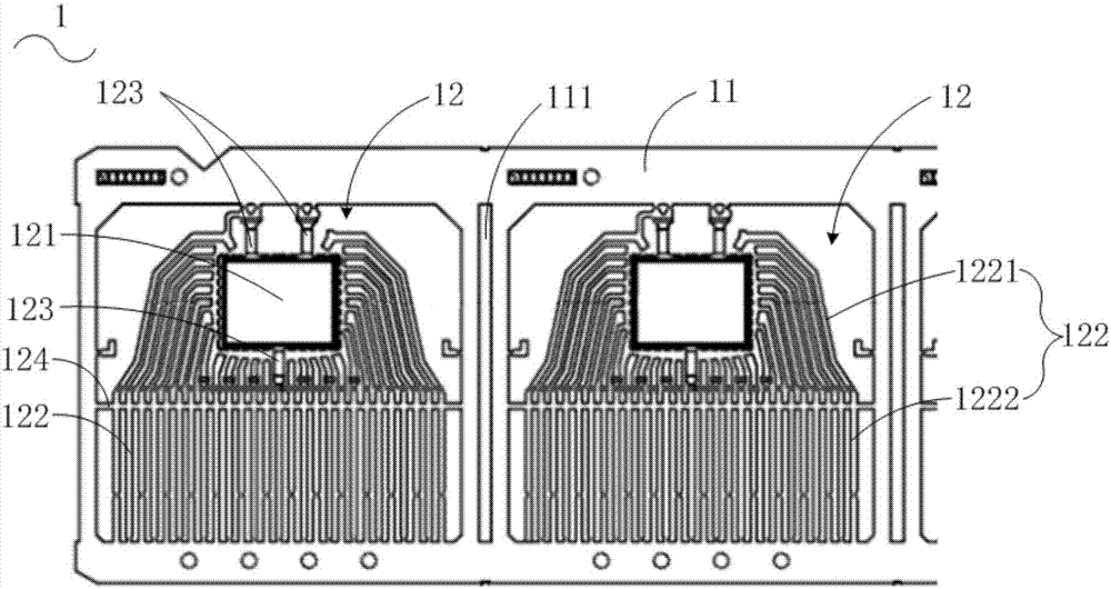
[0026] refer to figure 1 , the lead frame 1 of the preferred embodiment of the present invention includes a frame 11 and a plurality of chip packaging units 12 sequentially arranged along the length direction of the frame 11, and each chip packaging unit 12 is isolated from each other. The lead frame 1 is an integral structure, which is formed by punching and removing excess parts from a sheet base material, and the peripheral structure of the chip packaging unit 12 is the frame 11 .

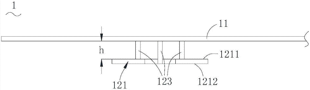
[0027] Preferably, in this embodiment, the frame 11 has a separation ...


PUM


Abstract

The invention provides a lead frame, a semiconductor device and a packaging technology of the semiconductor device. The lead frame comprises a border and multiple chip packaging units arranged in the border in the length direction of the border; each chip packaging unit comprises a chip base island, multiple pins and multiple splice bars connecting the chip base island with the border; all the pins and the border are located on the same plane, a height variation exists between the chip base island and the plane where the border is located, and then after packaging is conducted, the back surface of the chip base island can be exposed for cooling. According to the lead frame, a cooling fin in the prior art is omitted, the cost performance is high, correspondingly, the process of riveting the cooling pin in the prior art is omitted in the lead frame manufacturing process, and the defect that poor contact is caused by riveting is overcome; when the lead frame is packaged, the possibility that soldering tin is splashed to the pins can be lowered, and the frequency of occurrence of open circuit and short circuit is lowered; in addition, the fins can be clamped and fixed from the two sides of the pins for wire soldering, wire soldering is more stable, and the reliability of the product quality is improved.

Description

technical field [0001] The invention relates to the field of semiconductors, in particular to a lead frame, a semiconductor device and a packaging process for the semiconductor device. Background technique [0002] As a chip carrier, a lead frame generally has a plurality of chip packaging units, each chip packaging unit has a pin area and a chip area, and each chip packaging unit forms a semiconductor device by adding a chip and packaging it. For semiconductor devices such as power amplifiers, the lead frame in the traditional Flexiwatt packaging form is composed of two parts: a heat sink and a frame that are separated; the frame carries the lead function, and multiple pin areas are formed on it, and each pin in the pin area A hollow area is enclosed between the inner ends; the heat sink carries the chip mounting and heat dissipation functions, and is set corresponding to the pin area, and each heat sink is combined with a corresponding pin area to form a chip packaging uni...

Claims


Application Information

Patent Timeline
Patent Type & Authority Applications(China)
IPC IPC(8): H01L23/495
CPCH01L23/49503H01L23/49548H01L23/49568
Inventor 陈中溧林国志杨卫华游志涛
Owner SHENZHEN STS MICROELECTRONICS
Why Eureka
Try Eureka