Silicon carbide power device with buried n-type channel and manufacturing method thereof
A power device, silicon carbide technology, applied in semiconductor/solid-state device manufacturing, semiconductor devices, electrical components, etc., can solve problems such as insufficient reliability, achieve the effect of improving stability and reliability, improving electric field distribution, and protecting devices
- Summary
- Abstract
- Description
- Claims
- Application Information
AI Technical Summary
Problems solved by technology
Method used
Image

Examples
Embodiment 1
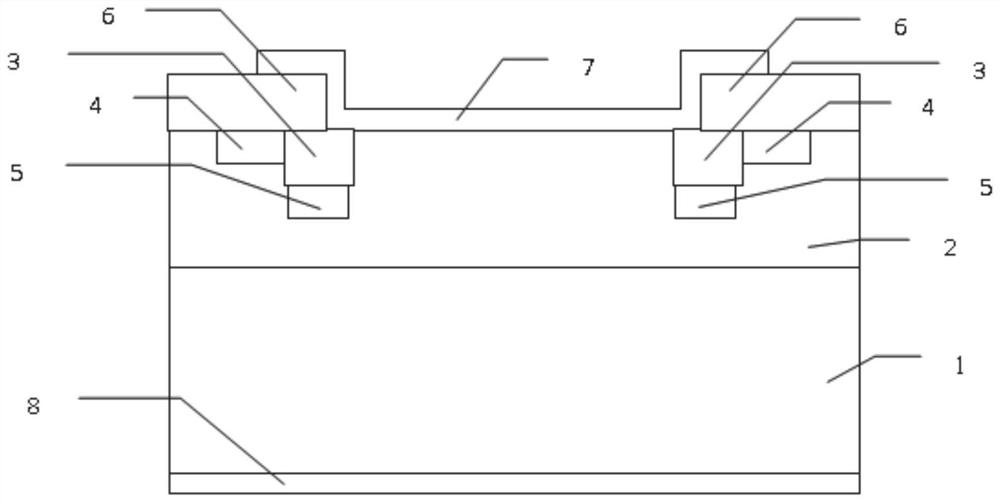
[0025] figure 1 It is a cross-sectional view of a silicon carbide power device with a buried N-type channel involved in Embodiment 1, combined below figure 1 The structure of the silicon carbide power device in Embodiment 1 will be described in detail.
[0026] Such as figure 1 As shown, the back metal contact 8 is arranged at the bottom, the back metal contact is an ohmic contact, and the metal type includes Ti, Al, Ni, Au, Ag, Pt, Wu and other metals, or some oxide metals.
[0027] A silicon carbide substrate 1 is provided above the metal contact 8 on the back surface, and an N-type silicon carbide substrate is used in this embodiment. A silicon carbide epitaxial layer 2 is disposed above the silicon carbide substrate 1 , and this embodiment uses an N-type silicon carbide epitaxial layer.
[0028] An active injection region 3 , a JTE injection region 4 and an N-type buried channel 5 are set in the silicon carbide epitaxial layer 2 . The active implantation region 3 of th...
Embodiment 2
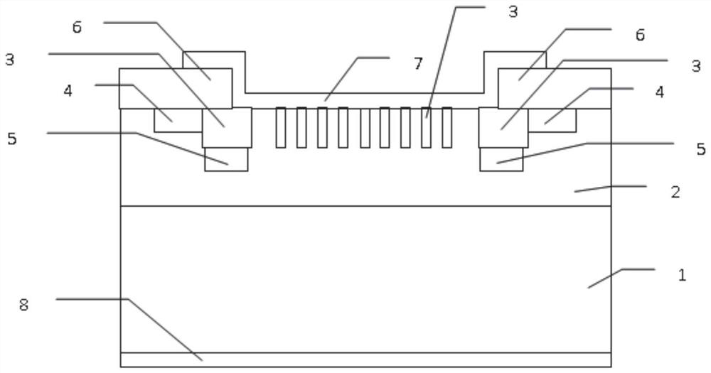
[0042] figure 2 It is a cross-sectional view of a silicon carbide power device with a buried N-type channel involved in Embodiment 2, combined below figure 2 The structure of the silicon carbide power device of the second embodiment will be described in detail.
[0043] Such as figure 2 As shown, the back metal contact 8 is arranged at the bottom, the back metal contact is an ohmic contact, and the metal type includes Ti, Al, Ni, Au, Ag, Pt, Wu and other metals, or some oxide metals.
[0044] A silicon carbide substrate 1 is provided above the metal contact 8 on the back surface, and an N-type silicon carbide substrate is used in this embodiment. A silicon carbide epitaxial layer 2 is disposed above the silicon carbide substrate 1 , and this embodiment uses an N-type silicon carbide epitaxial layer.
[0045] An active injection region 3 , a JTE injection region 4 and an N-type buried channel 5 are set in the silicon carbide epitaxial layer 2 . The active implantation re...
PUM
| Property | Measurement | Unit |
|---|---|---|
| thickness | aaaaa | aaaaa |
| thickness | aaaaa | aaaaa |
Abstract
Description
Claims
Application Information
 - R&D
- Intellectual Property
- Life Sciences
- Materials
- Tech Scout
- Unparalleled Data Quality
- Higher Quality Content
- 60% Fewer Hallucinations
Browse by: Latest US Patents, China's latest patents, Technical Efficacy Thesaurus, Application Domain, Technology Topic, Popular Technical Reports.
© 2025 PatSnap. All rights reserved.Legal|Privacy policy|Modern Slavery Act Transparency Statement|Sitemap|About US| Contact US: help@patsnap.com