PZT/Si diffusion bonding method

A diffusion bonding and bonding technology, applied in piezoelectric/electrostrictive/magnetostrictive devices, electrical components, circuits, etc., can solve the problems of difficult operation, complicated transfer bonding process, etc. Commercial promotion and application, low cost effect

Active Publication Date: 2017-12-15
DALIAN UNIV OF TECH
View PDF4 Cites 0 Cited by
  • Summary
  • Abstract
  • Description
  • Claims
  • Application Information

AI Technical Summary

Problems solved by technology

Thinning the PZT bulk material to 100 μm is already the limit of mechanical processing, and the y

Method used


Image

  • PZT/Si diffusion bonding method
  • PZT/Si diffusion bonding method

Examples


Embodiment Construction

[0029] The specific implementation manners of the present invention will be described in detail below in conjunction with the technical solutions and accompanying drawings.

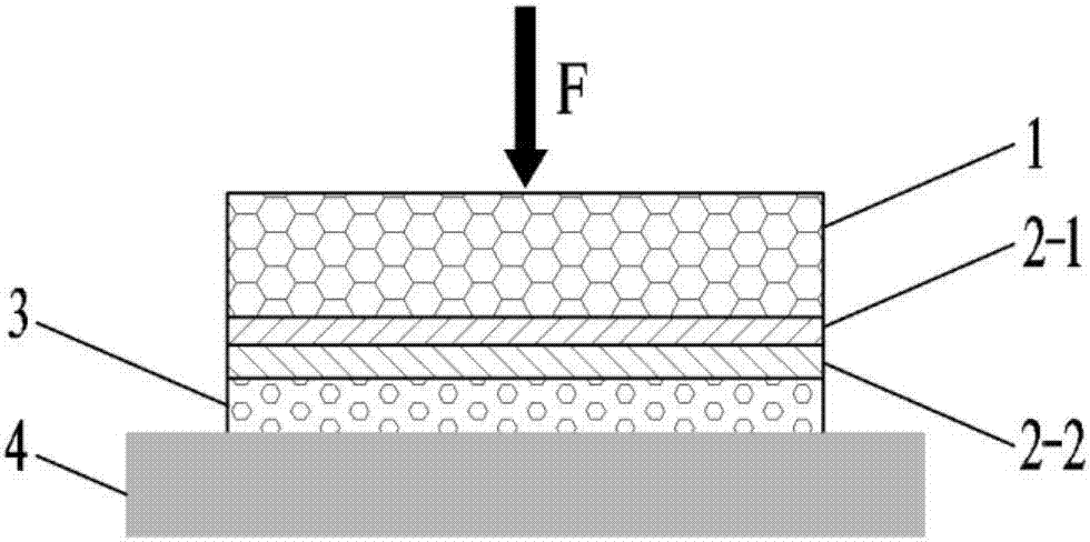
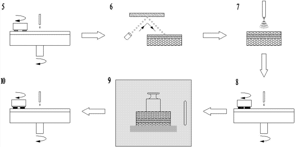
[0030] Firstly, the PZT block is ground, polished, and degreased; then, the Ti electrode and the Pt electrode are sputtered on the surface of the PZT block, and a certain thickness of PZT film is deposited on the surface of the Pt electrode. The PZT block and electrode layer and a PZT film constitute a PZT element. The PZT / Si diffusion bonding process is: under certain temperature conditions, by applying pressure to the PZT element and the silicon substrate, the PZT film and the silicon are diffusely bonded to achieve a stable combination of the PZT element / silicon; Grinding and polishing process to obtain PZT piezoelectric layer of desired thickness.

[0031] The concrete implementation steps of embodiment are as follows:

[0032] 1) Surface pretreatment of PZT blocks

[0033] In this embodiment, the ...


PUM

PropertyMeasurementUnit
Surface roughnessaaaaaaaaaa
Roughnessaaaaaaaaaa
Surface roughnessaaaaaaaaaa

Abstract

The present invention belongs to the field of advanced manufacturing technology and provides a PZT/Si diffusion bonding method. First, an electrode layer is prepared on the surface of a PZT bulk material, and a PZT film is deposited on the surface of the electrode layer to form a PZT device. Then, under certain temperature conditions, through the exertion of pressure on the PZT device and the silicon substrate, the lead and the silicon elements in the PZT film are subjected to a diffusion reaction to form a diffusion bonding layer with a certain depth and a high bonding force. In this way, the stable and solid combination of the PZT device with the silicon is realized. Finally, a PZT piezoelectric layer with required thickness is obtained by the subsequent mechanical grinding and polishing process. The PZT/Si bonding mode achieves a high bonding strength, is simple to process, and convenient to implement. Low in cost, the method is favorable for commercial popularization and application.

Description

technical field [0001] The invention belongs to the field of advanced manufacturing technology and provides a PZT / Si diffusion bonding method. Background technique [0002] In recent years, Micro-Electro-Mechanical Systems (MEMS), which integrates information collection, processing, and execution, has been highly regarded by academia and industry for its advantages of miniaturization, low energy consumption, high sensitivity, and high integration. focus on. [0003] Piezoelectric materials have the characteristics of mutual conversion of electrical energy and mechanical energy. Piezoelectric MEMS devices (pMEMS) such as sensors, actuators, and energy harvesters made of piezoelectric materials have become an important branch of MEMS research. Among them, silicon-based pMEMS devices dominate. Lead zirconate titanate (PZT) piezoelectric ceramic material has a relatively high piezoelectric coefficient d 33 , and are widely used in silicon-based piezoelectric devices. [0004...

Claims


Application Information

Patent Timeline
IPC IPC(8): H01L41/312
CPCH10N30/072
Inventor 王大志石鹏慈元达周鹏凌四营任同群梁军生韦运龙
Owner DALIAN UNIV OF TECH
Why Eureka
Try Eureka