Array substrate, manufacturing method thereof and liquid crystal display panel

A technology of array substrate and substrate substrate, which is applied in transistors, semiconductor/solid-state device manufacturing, optics, etc., and can solve problems such as interface defects

Active Publication Date: 2017-12-29
TCL CHINA STAR OPTOELECTRONICS TECH CO LTD
View PDF4 Cites 1 Cited by
  • Summary
  • Abstract
  • Description
  • Claims
  • Application Information

AI Technical Summary

Problems solved by technology

[0004] In the long-term research and development process, the inventors of the present application found that the common electrode in the current FFS liquid crystal display is usually arranged above the source layer and the drain layer, and the lightly doped drain structure is usually formed by ion implantation. The interface is flawed

Method used


Image

  • Array substrate, manufacturing method thereof and liquid crystal display panel
  • Array substrate, manufacturing method thereof and liquid crystal display panel
  • Array substrate, manufacturing method thereof and liquid crystal display panel

Examples


Embodiment Construction

[0041] The following will clearly and completely describe the technical solutions in the embodiments of the present invention in conjunction with the accompanying drawings in the embodiments of the present invention. Obviously, the described embodiments are only some of the embodiments of the present invention, not all of them. Based on the embodiments of the present invention, all other embodiments obtained by persons of ordinary skill in the art without making creative efforts belong to the protection scope of the present invention.

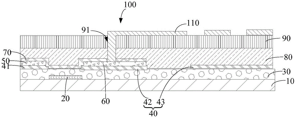
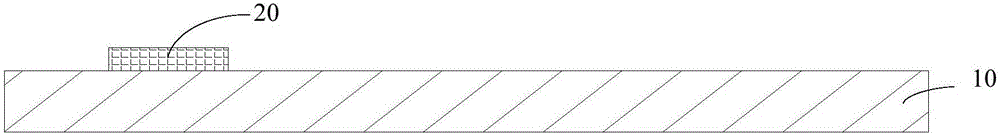
[0042] see figure 1 , the present invention provides an array substrate 100 according to an embodiment, which is used in a liquid crystal display panel. The array substrate 100 includes: a base substrate 10, a gate layer 20, a gate insulating layer 30, a common electrode layer 40, a source layer 50 and a drain layer 60, a metal oxide semiconductor material layer 70, a passivation layer 80, A flat layer 90 and a pixel electrode layer 110 .

[...


PUM

PropertyMeasurementUnit
thicknessaaaaaaaaaa
thicknessaaaaaaaaaa
thicknessaaaaaaaaaa

Abstract

The invention provides an array substrate, a manufacturing method thereof and a liquid crystal display panel. The array substrate comprises the components of a substrate; a gate electrode layer; a gate electrode insulating layer; a common electrode layer which comprises a first common electrode layer, a second common electrode layer and a third common electrode layer, wherein the first common electrode layer and the second common electrode layer are arranged at two ends of the gate electrode layer; a source electrode layer and a drain electrode layer; a metal oxide semiconductor material layer which covers the source electrode layer, the gate electrode insulating layer and the drain electrode layer, wherein the transparent electrode material of the first common electrode layer and the second common electrode layer and metal oxide semiconductor material of the metal oxide semiconductor material layer form a lightly doped drain structure LDD in a mutual contact area; a passivation layer; a flat layer; and a pixel electrode layer. Through the array substrate, the manufacturing method thereof and the liquid crystal display panel, the lightly doped drain structure LDD can be formed in a non-ion-injection manner, thereby eliminating interface defects.

Description

technical field [0001] The invention relates to the field of display technology, in particular to an array substrate, a manufacturing method thereof, and a liquid crystal display panel. Background technique [0002] In an in-plane switching (In-Plane Switching, IPS) mode liquid crystal display, when the liquid crystal molecules are arranged outside the pixel electrode and the common electrode, they cannot be driven but maintain the initial state, that is, maintain the initial alignment direction. Since the liquid crystal molecules cannot properly control the light transmittance in the initial state, the aperture ratio and brightness will be reduced. [0003] At present, in order to solve the above-mentioned shortcomings of the IPS mode liquid crystal display, a fringe field switching (Fringe Field Switching, FFS) type liquid crystal display driven by a fringe electric field has been proposed. The FFS type liquid crystal display includes a common electrode and a pixel electr...

Claims


Application Information

Patent Timeline
Patent Type & Authority Applications(China)
IPC IPC(8): H01L27/12H01L29/78H01L29/786H01L21/84H01L21/34G02F1/1343G02F1/1362G02F1/1368
CPCG02F1/1343G02F1/13439G02F1/136227G02F1/1368G02F1/134372G02F1/136295H01L27/124H01L27/1288H01L29/66969H01L29/7833H01L29/7869
Inventor 李金明
Owner TCL CHINA STAR OPTOELECTRONICS TECH CO LTD
Why Eureka
Try Eureka