Preparation method of compound semiconductor device and compound semiconductor device

A semiconductor and compound technology, applied in the fields of semiconductor/solid-state device manufacturing, semiconductor devices, semiconductor/solid-state device components, etc., can solve the problems of quantum well layer source region defects, performance damage, photoelectric and signal crosstalk, etc., to avoid Signal crosstalk, the effect of improving performance

Inactive Publication Date: 2021-09-28
格芯致显杭州科技有限公司
View PDF1 Cites 1 Cited by
  • Summary
  • Abstract
  • Description
  • Claims
  • Application Information

AI Technical Summary

Problems solved by technology

[0007] 1) if Figure 1A As shown, the device is prepared by a selective area growth scheme. When the actual material is grown, there will be defects in the material in the area around the masking layer 120, resulting in defects in the active region of the quantum well layer, and problems such as performance damage;
[0008] 2) The device shares the first semiconductor layer 110 (that is, the common pole through the first semiconductor layer 110), and there will be photoelectric and signal crosstalk problems between the devices due to the common use of the first semiconductor layer 110;

Method used


Image

  • Preparation method of compound semiconductor device and compound semiconductor device
  • Preparation method of compound semiconductor device and compound semiconductor device
  • Preparation method of compound semiconductor device and compound semiconductor device

Examples


preparation example Construction

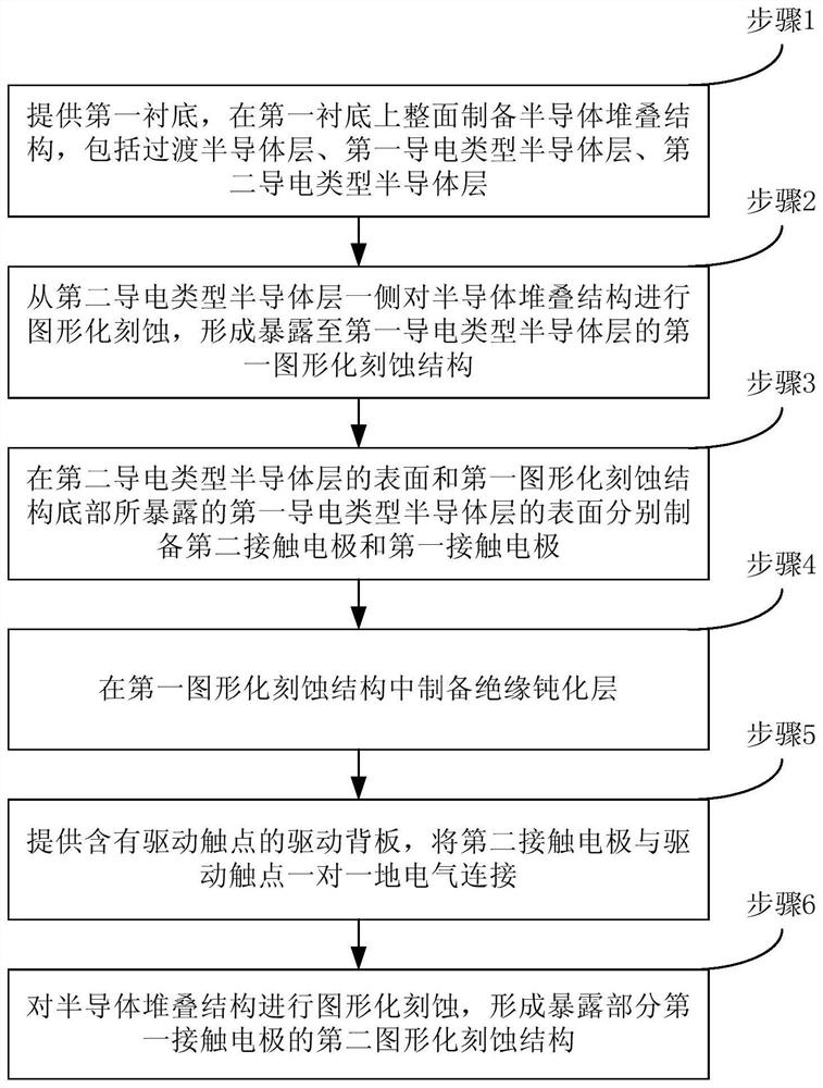
[0091] like figure 2 As shown, the method for preparing a compound semiconductor device provided by the embodiment of the present invention mainly includes the following steps:

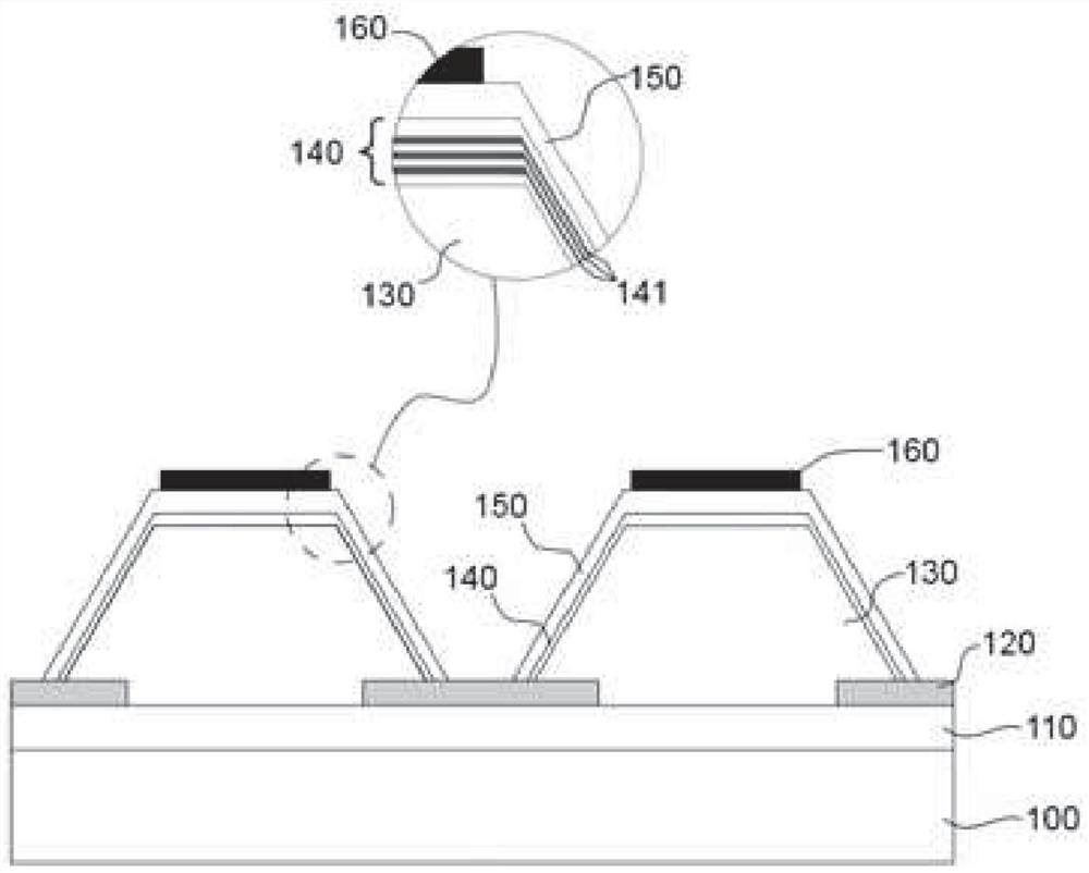
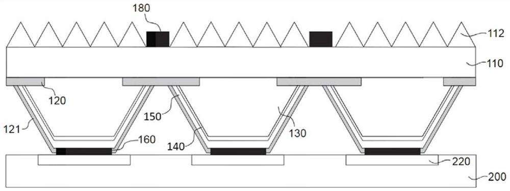
[0092] Step 1. Provide a first substrate, and prepare a semiconductor stack structure on the entire surface of the first substrate. The semiconductor stack structure includes a transition semiconductor layer stacked outward from the surface of the first substrate, a first conductivity type semiconductor layer, a second conductivity type type semiconductor layer;

[0093] Step 2: Perform patterned etching on the semiconductor stack structure from the side of the semiconductor layer of the second conductivity type to form a first patterned etched structure exposed to the semiconductor layer of the first conductivity type, wherein the first patterned etched structure penetrates The second conductivity type semiconductor layer does not penetrate through the first conductivity type semiconductor layer; ...


PUM

PropertyMeasurementUnit
thicknessaaaaaaaaaa
thicknessaaaaaaaaaa
thicknessaaaaaaaaaa

Abstract

The invention discloses a preparation method of a compound semiconductor device and the compound semiconductor device. The preparation method mainly comprises the following steps of preparing a first conductive type semiconductor layer and a second conductive type semiconductor layer on the whole surface of a substrate, performing graphical etching from one side of the second conductive type semiconductor layer to form a first graphical etching structure exposed to the first conductive type semiconductor layer, respectively preparing a second contact electrode and a first contact electrode on the surface of the second conductive type semiconductor layer and the surface of the first conductive type semiconductor layer at the bottom of the first graphical etching structure, preparing an insulating passivation layer in the first graphical etching structure, electrically connecting the second contact electrode with the driving contact, and forming a second graphical etching structure which exposes a part of the first contact electrode from one side of the first conductive type semiconductor layer. The defects of the material layer caused by selected area growth do not exist, signal crosstalk between devices can be avoided, and the performance of the compound semiconductor device can be improved on the whole.

Description

technical field [0001] The invention relates to the field of semiconductor device manufacturing, in particular to a method for preparing a monolithically integrated compound semiconductor device and the monolithically integrated compound semiconductor device. Background technique [0002] In traditional semiconductor systems, functional devices or devices and drive circuits are often separated on different wafers or substrates, or distributed in different regions of the same wafer or substrate, and electrical function-related connections are realized by related wiring. For example, after the compound semiconductor device is prepared, it is packaged on a PCB (Printed Circuit Board, printed circuit board) circuit or a CMOS (Complementary Metal Oxide Semiconductor, complementary metal oxide semiconductor) driver. This type of wiring may generate more impedance and electromagnetic interference due to length and distance issues, which affects energy consumption and signal transmi...

Claims


Application Information

Patent Timeline
Patent Type & Authority Applications(China)
IPC IPC(8): H01L21/48H01L23/48H01L23/485
CPCH01L21/4846H01L23/48H01L23/485
Inventor 李勇
Owner 格芯致显杭州科技有限公司
Why Eureka
Try Eureka