Method for preparing optical super-structure surface based on nanoimprinting

A metasurface, nano-imprinting technology, applied in nano-optics, originals for opto-mechanical processing, optics, etc., can solve the problems of long preparation time and high cost, optimize production process, save production cost, and low cost Effect

Inactive Publication Date: 2018-01-09
深圳南科构彩科技有限公司
View PDF4 Cites 26 Cited by
  • Summary
  • Abstract
  • Description
  • Claims
  • Application Information

AI Technical Summary

Problems solved by technology

[0005] In view of the above-mentioned problems existing in the prior art, the object of the present invention is to provide a method for preparing an optical metasurface based on nanoimprinting to solve the problems of long preparation time and high cost in the prior art

Method used


Image

  • Method for preparing optical super-structure surface based on nanoimprinting
  • Method for preparing optical super-structure surface based on nanoimprinting
  • Method for preparing optical super-structure surface based on nanoimprinting

Examples


Embodiment 1

[0080] This embodiment provides a method for preparing an optical metasurface optical device based on nanoimprinting, the specific method is:

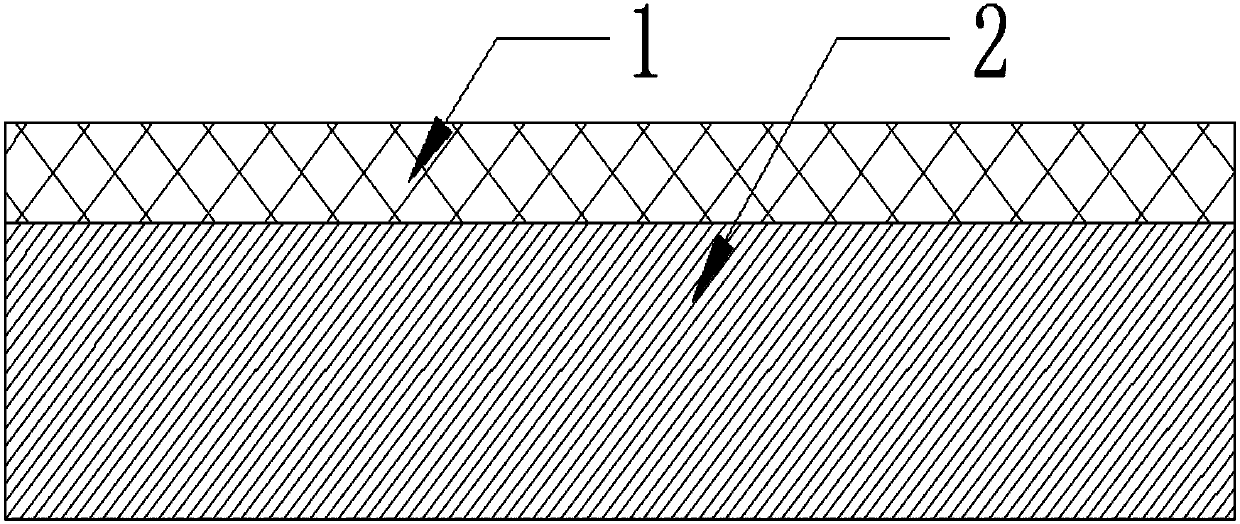
[0081] a. Spin-coat a layer of electron beam lithography positive resist 1 with a thickness of about 150 nm on the silicon wafer 2 (the schematic diagram of the product is as follows Figure 1.1 shown);

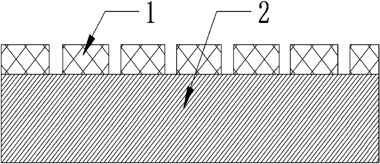
[0082] b. Use electron beam lithography to write the designed metasurface functional element pattern, and develop it with a developer (the schematic diagram of the product is as follows Figure 1.2 shown);

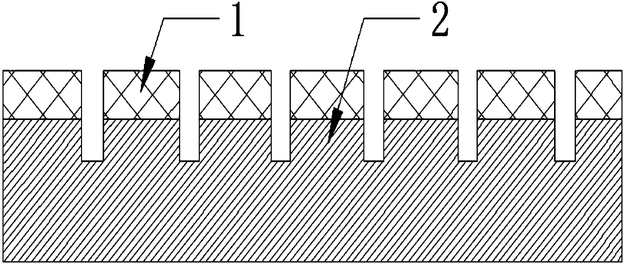
[0083] c. Use the electron beam lithography positive resist 1 as a mask to perform ICP etching on the silicon wafer 2, and the etching depth is about 200nm (the schematic diagram of the product is as follows Figure 1.3 shown);

[0084] d. Remove the electron beam photoresist positive resist 1 with the corresponding solvent (the schematic diagram of the product is as follows Figure 1.4 shown);

[0085] e. Evaporate a layer of...

Embodiment 2

[0094] This embodiment provides a method for preparing an optical metasurface optical device based on nanoimprinting, the specific method is:

[0095] a. With reference to the four steps of a, b, c, and d in Example 1, a silicon wafer 9 with a designed metasurface functional element pattern is prepared (the schematic diagram of the product is as follows Figure 2.1 shown);

[0096] b. transfer the pattern on the silicon wafer 9 with the designed metasurface functional primitive pattern to the polymer film 10 (such as PC, PMMA, PEEK, PI, PET, PU, ​​PTFE, PVDF or PDMS, etc.) (the schematic diagram of the product is as Figure 2.2 shown);

[0097] c. The polymer film 10 is separated from the silicon wafer 9, and the pattern on the silicon wafer 9 is transferred to the polymer film 10 to complete the production of the nanoimprint template (the schematic diagram of the product is as follows Figure 2.3 shown);

[0098] d. On the substrate 7 (the substrate 7 is a silicon substrate...

Embodiment 3

[0102] This embodiment provides a method for preparing an optical metasurface optical device based on nanoimprinting, the specific method is:

[0103] a. On the transparent substrate 13, spin-coat a layer of nano-imprint glue 12 with good adhesion to the transparent substrate, and use the Ni metal imprint template or macromolecule with a designed superstructure surface functional element pattern Thin film imprinting template 11 (the material of the polymer film is PC, PMMA, PEEK, PI, PET, PU, ​​PTFE, PVDF or PDMS, etc.) presses the nanoimprinting glue 12, and transfers the pattern to the nanoimprinting glue 12 (product schematic diagram Such as Figure 3.1 shown), the specific transfer process and the cleaning process after the transfer can refer to steps h and i of Example 1;

[0104] b. Utilize the nano-imprint glue 12 as a mask to etch the transparent substrate 13, and the etching depth is the thickness of the metal layer of the designed metasurface functional element (the...


PUM

PropertyMeasurementUnit
thicknessaaaaaaaaaa
thicknessaaaaaaaaaa
thicknessaaaaaaaaaa

Abstract

The invention discloses a method for preparing an optical super-structure surface based on nanoimprinting. According to the method, an adopted template is an impressing template with a super-structurefunctional element pattern. The method for preparing the optical super-structure surface based on the nanoimprinting, provided by the invention, can be used for replacing an electron beam lithographymethod when preparing a super-structure functional element, the cost is reduced by a large margin and the production time is shortened. According to the method provided by the invention, the production cost is remarkably reduced, and the production time is remarkably shortened, thus the low-cost and large-scale manufacturing of a super-structure surface optical element within a short time is realized, and good industrial prospect is realized.

Description

technical field [0001] The invention relates to the field of micro-nano processing, in particular to the preparation of optical metasurfaces. Background technique [0002] Optical metamaterials are artificially engineered optical structural materials in which metaunits allow light to propagate in a way that is impossible in natural materials. We can design the linear optical parameters of metamaterials, such as effective permittivity, magnetic permeability, refractive index, etc., by adjusting the constituent materials and geometric shapes of metaunits. In this way, the electromagnetic response of the metaunit is no longer limited by its own chemical composition. By rationally designing optical metamaterials, we can realize some exotic optical physical phenomena, such as negative refraction, super-resolution imaging, and optical cloaking. However, the challenges encountered in nanofabrication of 3D metamaterials and its huge optical loss limit its practical application in ...

Claims


Application Information

Patent Timeline
Patent Type & Authority Applications(China)
IPC IPC(8): G03F7/00G03F7/039
CPCG03F7/0002G03F7/2037G03F7/40G03F7/0005B82Y40/00B82Y20/00G02B1/002G03F1/60G03F1/78G03F7/033
Inventor 程鑫李贵新庄鑫邓俊鸿
Owner 深圳南科构彩科技有限公司
Why Eureka
Try Eureka