
Production method of metallized semi-hole of printed circuit board

A metallized half-hole, printed circuit board technology, applied in the direction of printed circuit manufacturing, printed circuit, electrical components, etc., can solve the problems of long process and high quality risk, and achieve the goal of improving production efficiency, shortening the production process and reducing production costs Effect

Inactive Publication Date: 2018-01-12
珠海精毅电路有限公司
View PDF2 Cites 6 Cited by
  • Summary
  • Abstract
  • Description
  • Claims
  • Application Information

AI Technical Summary

Problems solved by technology

[0003] The purpose of the present invention is to provide a method for making metallized semi-holes in circuit boards that solves the problem of sharp edges and burrs in view of the shortcomings of the prior art, such as long process flow and high quality risk.

Method used

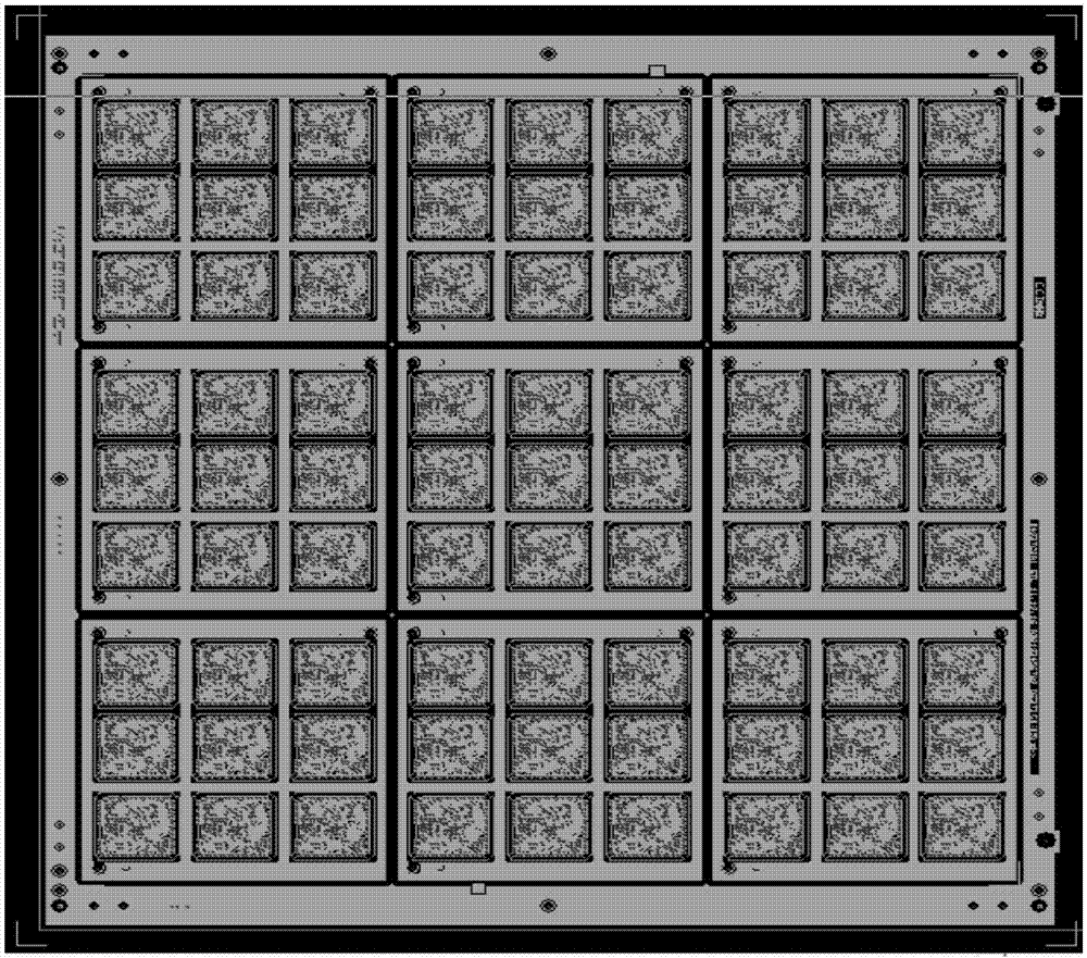
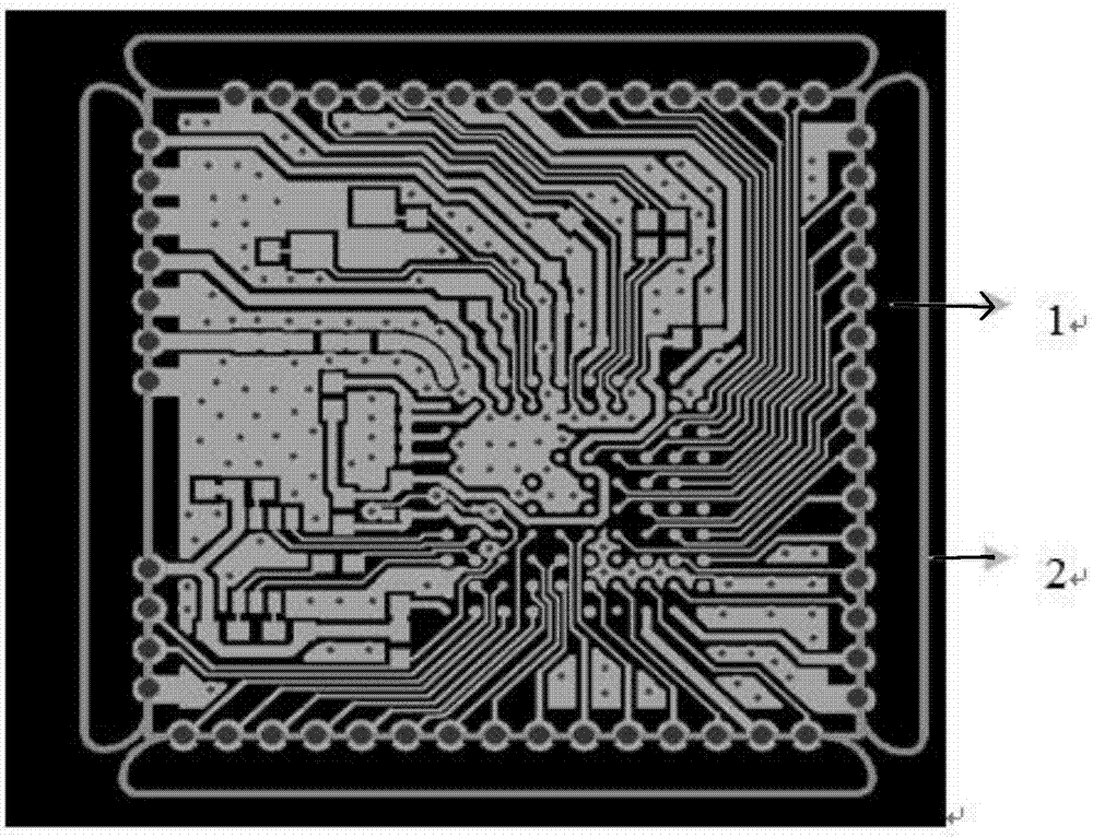

Image

  • Production method of metallized semi-hole of printed circuit board
  • Production method of metallized semi-hole of printed circuit board
  • Production method of metallized semi-hole of printed circuit board

Examples


Embodiment Construction

[0014] The present invention and its beneficial effects will be further described in detail below in conjunction with specific embodiments, however, the specific embodiments of the present invention are not limited thereto.

[0015] This embodiment provides a method for manufacturing a metallized half-hole on a printed circuit board, which includes the following steps:

[0016] A. Complete the production process of the circuit board from material cutting to surface treatment, and form a half-hole production state board to be metallized: material cutting, baking plate, inner layer circuit, inner layer etching, inner layer AOI, pressing, edge milling, drilling Hole, electroplating, outer layer circuit, outer layer acid etching, outer layer AOI, solder mask, text, immersion nickel gold / spray tin, etc. before milling and metallizing the half hole;

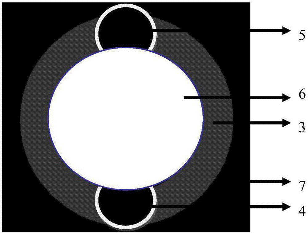
[0017] B. Design the second drill drill belt, drill a hole 4 and 5 with a diameter of 1.0mm on both sides of the hole where the metal...


PUM


Abstract

The invention provides a production method of a semi-hole of a printed circuit board. The method comprises the following steps that a, process production of the circuit board from cutting to surface treatment is completed to form a semi-hole production state board to be metallized; b, secondary drilling is conducted on the portions, on the two sides of the metallized semi-hole, of the hole wall, wherein the circuit board is fixed to a drilling machine through locating nails, a drill bit cuts in the hole wall in a rotating mode clockwise, that is to say, small holes are drilled in the portions,on the two sides of the semi-hole in the position to be milled later, of the hole wall, and hole wall copper is drilled to be broken; c, board edge milling is conducted on the metallized semi-hole, wherein a board milling program is acquired, the metallized hole edge is milled by a milling cutter clockwise to achieve a board milling movement, and the metallized semi-hole is formed; d, board milling is conducted on the unit edge, wherein the board milling program is acquired, the unit edge is milled according to normal operation parameters to achieve a board milling movement, the circuit boardis milled to small units, and a production board with the metallized semi-hole is formed. By means of the production method of the semi-hole of the printed circuit board, the burr problem is solved,the production process of the circuit board is shortened, the production cost is lowered, and the quality, the yield and the production efficiency are improved.

Description

technical field [0001] The invention relates to the field of manufacturing printed circuit boards, in particular to a method for manufacturing metallized half holes of printed circuit boards. Background technique [0002] In the production of printed circuit boards, there are usually products that require a metallized half-hole design on the edge of the board. When this type of design is manufactured according to the traditional milling process, there is a problem of remaining edge. Specifically: when milling the metallized half hole, when the milling cutter enters the metallized half hole, the copper skin in the hole on the entrance side is in a state of no force support. When milling the plate, the copper skin on the side hole wall will follow the rotation of the milling cutter. It is involved in the hole to form a burr peak; on the other side of the hole, because of the support of the hole wall, the copper skin is milled off, and there is no burr peak. In order to preven...

Claims


Application Information

Patent Timeline
Patent Type & Authority Applications(China)
IPC IPC(8): H05K3/00
Inventor 唐令新
Owner 珠海精毅电路有限公司
Learn More