Organic light emitting diode substrate and manufacturing method therefor

A technology of light-emitting diodes and substrates, which is applied in the fields of organic semiconductor devices, semiconductor/solid-state device manufacturing, electrical components, etc., and can solve problems such as uneven voltage distribution, viewing angle deviation, and low cathode transmittance

Active Publication Date: 2018-01-19
BOE TECH GRP CO LTD +1
View PDF18 Cites 21 Cited by
  • Summary
  • Abstract
  • Description
  • Claims
  • Application Information

AI Technical Summary

Problems solved by technology

For example, in order to meet the requirements of light transmittance, the thickness of the cathode must be thinner, but at this time the resistance of the cathode is relatively large, which will not only lead to problems of voltage rise and power consumption, but also cause uneven voltage distribution on the cathode. There is a problem with uneven brightness
In order to meet the conductivity requirements, the thickness of the cathode must be relatively large, but at this time the transmittance of the cathode is low, and there will be a problem of angular deviation

Method used


Image

  • Organic light emitting diode substrate and manufacturing method therefor
  • Organic light emitting diode substrate and manufacturing method therefor
  • Organic light emitting diode substrate and manufacturing method therefor

Examples


preparation example Construction

[0052] In order to simultaneously improve the light transmittance and conductivity of the top emission OLED, an embodiment of the present application provides a method for manufacturing an organic light emitting diode substrate. figure 1 It is a flowchart of a method for preparing an organic light emitting diode substrate according to an embodiment of the present invention. like figure 1 As shown, the preparation method of the organic light emitting diode substrate includes:

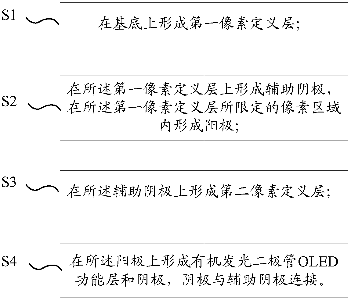
[0053] S1. Forming a first pixel definition layer on a substrate;

[0054] S2. Forming an auxiliary cathode on the first pixel definition layer, and forming an anode in a pixel region defined by the first pixel definition layer;

[0055] S3. Forming a second pixel definition layer on the auxiliary cathode;

[0056] S4, forming an OLED functional layer and a cathode on the anode, and the cathode is connected to the auxiliary cathode.

[0057] Wherein, step S1 includes: depositing a pixel-defining film...

no. 1 example

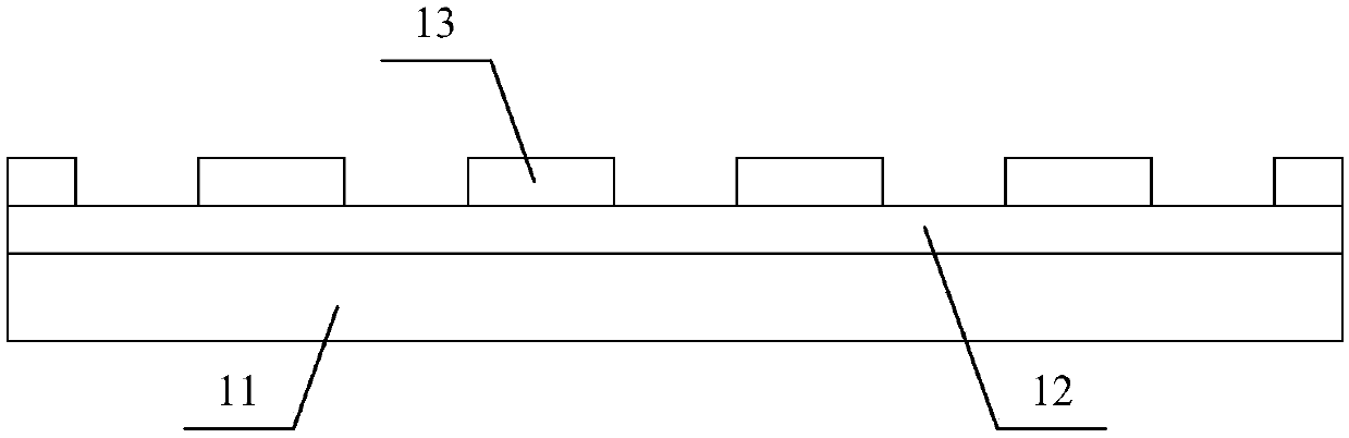
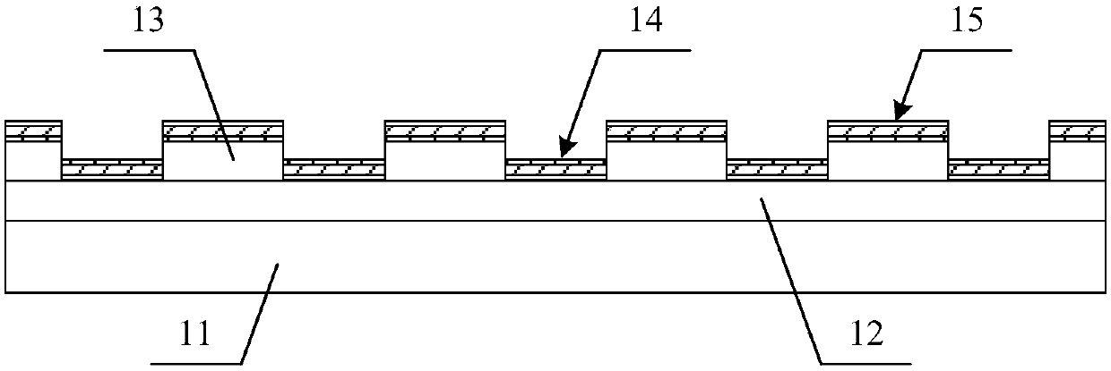
[0072] Figure 2-7 It is a schematic diagram of preparing an OLED substrate according to the first embodiment of the present invention. Combine below Figure 2-7 The method for preparing the organic light emitting diode substrate of this embodiment will be described in detail.

[0073] (1) Forming a pattern of the driving structure layer 12 on the substrate 11 through a patterning process. In this embodiment, the driving structure layer 12 includes a thin film transistor (Thin Film Transistor, TFT), and the structure and manufacturing process of the driving structure layer are the same as the existing manufacturing process. For example, the preparation process may include: cleaning the substrate first, and then sequentially preparing a gate electrode, an insulating layer, an active layer, a source-drain electrode and a flat layer on the substrate through a patterning process. The substrate material can be glass, quartz, polyethylene terephthalate (PET) or a surface-treated ...

no. 2 example

[0118] Figure 8 It is a schematic structural view of the OLED substrate according to the second embodiment of the present invention. The main structure of the OLED substrate of this embodiment is the same as that of the first embodiment, the difference is that the anode 14 and the auxiliary cathode 15 of this embodiment are only formed by a transparent conductive layer, and the thickness of the transparent conductive layer is 140-210 nm. Preferably, the thickness of the transparent conductive layer is 160-170 nm.

[0119] The process of preparing the organic light-emitting diode substrate in this embodiment is also similar to that of the first embodiment, the difference is that after the first pixel defining layer pattern is prepared, a transparent conductive layer is deposited by sputtering to form an anode 14 in the pixel area. pattern, the auxiliary cathode 15 pattern is formed on the first pixel defining layer, and the anode 14 and the auxiliary cathode 15 only include a...


PUM


Abstract

The invention provides an organic light emitting diode substrate and a manufacturing method therefor. The organic light emitting diode substrate comprises a pixel defining layer arranged on a substrate, and a positive electrode, an organic light emitting diode (OLED) functional layer and a negative electrode arranged in a pixel region; the pixel defining layer comprises a first pixel defining layer, an auxiliary negative electrode and a second pixel defining layer which are laminated in sequence; and the auxiliary negative electrode is connected with the negative electrode. By means of formingthe auxiliary negative electrode between the two pixel defining layers, forming the negative electrode in the pixel region and enabling the negative electrode to be connected with the auxiliary negative electrode, the problem of visual angle color error can be relieved effectively; in addition, the negative electrode voltage is uniform in distribution and relatively high luminance uniformity is achieved; and meanwhile, the transmission of light and conductivity of the OLED are improved.

Description

technical field [0001] The invention relates to the field of display technology, in particular to an organic light emitting diode substrate and a manufacturing method thereof. Background technique [0002] In the field of display technology, liquid crystal (Liquid Crystal Display, LCD) display devices and organic light emitting diode (Organic Light Emitting Diode, OLED) display devices have gradually replaced CRT displays. Due to the advantages of high brightness, saturated color, thinness, flexibility, and low cost, OLED display devices are expected to become the next-generation flat-panel display technology after LCD display technology, and are one of the most concerned technologies in flat-panel display technology. An active matrix organic light emitting diode (Active Matrix Organic Light Emitting Diode, AMOLED) display device is a type of OLED display device, and is mainly composed of a thin film transistor (Thin Film Transistor, TFT) and an OLED. [0003] According to ...

Claims


Application Information

Patent Timeline
Patent Type & Authority Applications(China)
IPC IPC(8): H01L51/52H01L51/56
CPCH10K59/122H10K50/13H10K50/816H10K50/824H10K50/828H10K2102/351H10K71/00H10K50/81H10K50/82H10K50/84H10K50/125H10K2102/3026
Inventor 吴海东李彦松杜小波
Owner BOE TECH GRP CO LTD
Why Eureka
Try Eureka