Si-doped InAs/GaAs quantum dot laser and preparation method thereof

A quantum dot and laser technology, which is applied in the field of Si-doped InAs/GaAs quantum dot laser and its preparation, can solve the problems of size, shape distribution uniformity and difficult control of density, and achieve the effect of reducing threshold current and improving device performance.

Inactive Publication Date: 2018-01-19
INST OF SEMICONDUCTORS - CHINESE ACAD OF SCI
View PDF2 Cites 6 Cited by
  • Summary
  • Abstract
  • Description
  • Claims
  • Application Information

AI Technical Summary

Problems solved by technology

The disadvantage of this method is that its size, shape, d

Method used


Image

  • Si-doped InAs/GaAs quantum dot laser and preparation method thereof
  • Si-doped InAs/GaAs quantum dot laser and preparation method thereof
  • Si-doped InAs/GaAs quantum dot laser and preparation method thereof

Examples


Embodiment 1

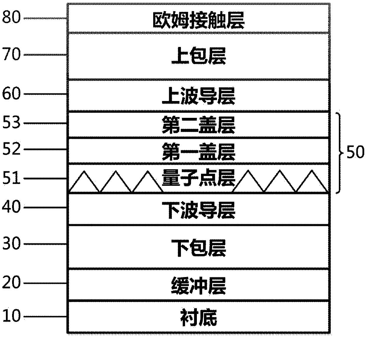
[0090] (1) Take a substrate 10, which is an n+ type GaAs substrate with a crystal orientation of (100), a doping element of Si, and a doping concentration of (0.5-5)×10 18 cm -3 ;

[0091] (2) Epitaxially grow a layer of GaAs buffer layer 20 on the above-mentioned GaAs substrate 10, the buffer layer growth thickness is 0-800nm, it is n-type doped, the doping element is Si element, and the doping concentration is (0.5- 5)×10 18 cm -3 ;

[0092] (3) Epitaxially grow the AlGaAs lower cladding layer 30 on the above-mentioned GaAs buffer layer 20, the growth thickness is 500-2000nm, and perform n-type doping on it, the doping element is Si element, and the doping concentration is (0.1-5)× 10 18 cm -3 ;

[0093] (4) epitaxially growing the GaAs lower waveguide layer 40 on the above-mentioned AlGaAs lower cladding layer 30, with a growth thickness of 50-200 nm;

[0094] (5) Epitaxially grow a Si-doped InAs quantum dot layer 51 on the above-mentioned GaAs lower waveguide layer...


PUM

PropertyMeasurementUnit
Doping concentrationaaaaaaaaaa
Growth thicknessaaaaaaaaaa
Thicknessaaaaaaaaaa

Abstract

The invention discloses a Si-doped InAs/GaAs quantum dot laser and a preparation method thereof. The Si-doped InAs/GaAs quantum dot laser is characterized by comprising a quantum dot active region (50), wherein the quantum dot active region (50) comprises a Si-doped quantum dot layer (51); and according to the preparation method of the quantum dot laser, a buffer layer (20), a lower cladding layer(30), a lower waveguide layer (40), the quantum dot active region (50), an upper waveguide layer (60), an upper cladding layer (70) and an ohmic contact layer (80) are sequentially grown on a substrate (10) by adopting an MBE epitaxial growth method. According to the quantum dot laser, a non-radiative recombination center near quantum dots is effectively passivated through introducing Si atoms and the optical property of a quantum dot material is strengthened; and meanwhile, threshold current of a laser device can be reduced through electrons introduced by the Si atoms and the performance ofthe device can be improved.

Description

technical field [0001] The invention belongs to the technical field of semiconductors, and in particular relates to a Si-doped InAs / GaAs quantum dot laser and a preparation method thereof. Background technique [0002] The continuous increase in the amount of information puts forward higher requirements for the light source of optical fiber communication. As the core component of the optical fiber communication system, the semiconductor laser plays a vital role in the performance of the whole system. Quantum dot materials have discrete energy levels similar to atoms, and the density of states is in the form of a delta function because the sizes in three dimensions are close to the de Broglie wavelength of electrons. Semiconductor quantum dot lasers exhibit superior characteristics such as low threshold current density, high differential gain, high temperature stability, high modulation rate, and low frequency chirp effect, and are expected to become important light sources ...

Claims


Application Information

Patent Timeline
IPC IPC(8): H01S5/343
Inventor 杨涛吕尊仁张中恺
Owner INST OF SEMICONDUCTORS - CHINESE ACAD OF SCI
Why Eureka
Try Eureka