Backlight source and application of OFED structure with composition of organic green light photoluminescence materials and organic red light photoluminescence materials
A photoluminescence and backlight technology, applied in the field of backlight with OFED structure, can solve the problems of inability to cover the NTSC color gamut, color reproduction degree and color purity difference, etc., to improve color purity, improve color rendering index, reduce The effect of energy loss
- Summary
- Abstract
- Description
- Claims
- Application Information
AI Technical Summary
Problems solved by technology
Method used
Image
Examples
Embodiment 1
[0072] An LCD display device comprising an LCD panel, an LED-based backlight module and a driver IC, wherein,
[0073] The LED-based backlight module includes a backplane, a backlight arranged on the backplane, and a diffusion plate arranged above the backlight:
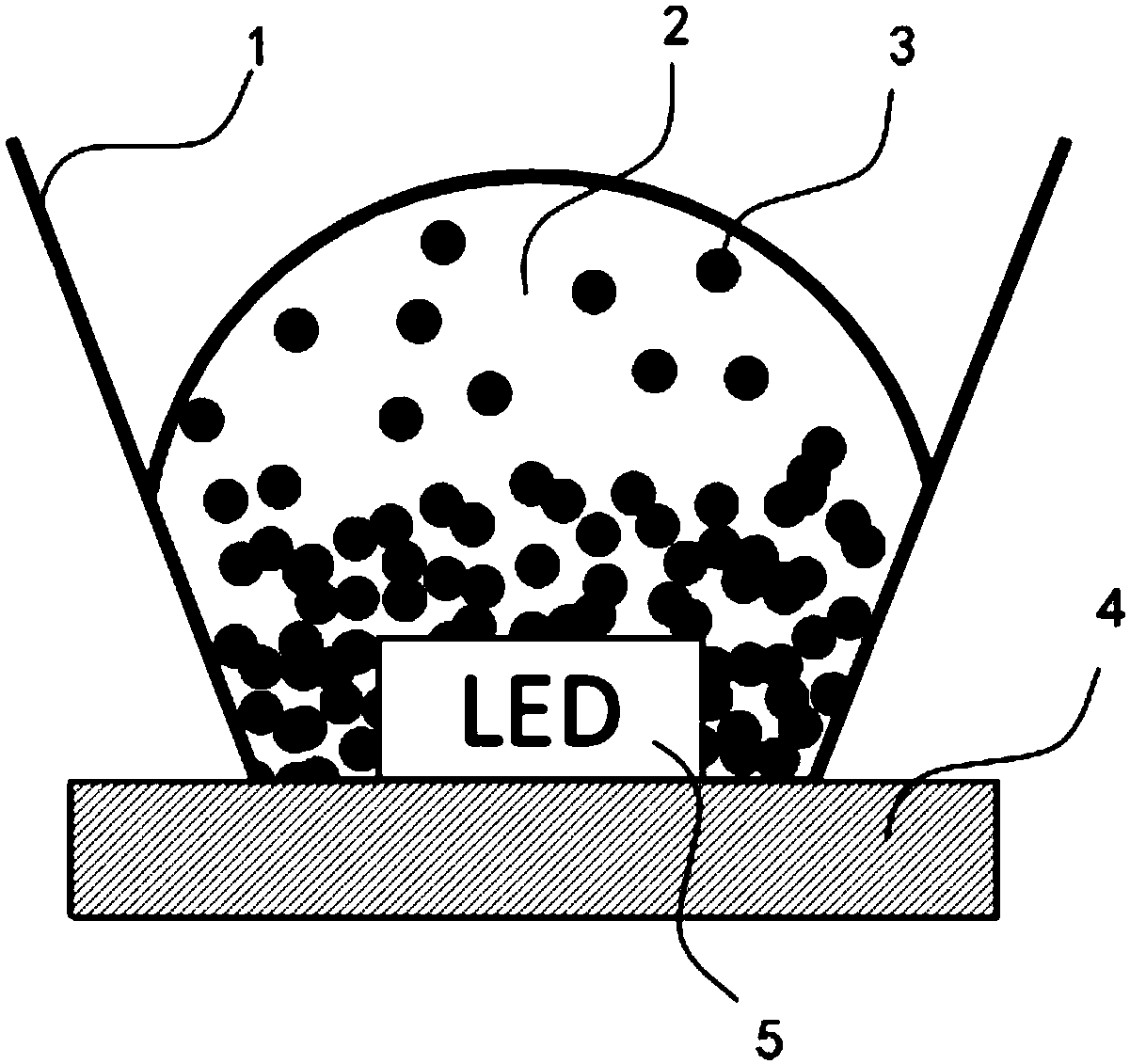
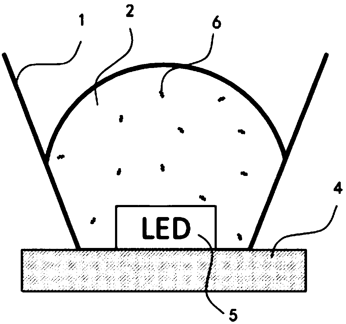
[0074] like figure 2 As shown, the backlight includes a PCB board 4 and an LED light emitting device arranged on the PCB board 4, and the LED light emitting device includes a blue LED chip 5 and a photoluminescent layer arranged above it;
[0075] The photoluminescent layer is an encapsulant 2 coated above the LED chip. The encapsulant 2 is loaded in the luminescent cup 1 with a coating thickness of 0.3 mm. The encapsulant 2 is evenly doped with organic green light. Photoluminescent materials and organic red photoluminescent materials3.
[0076] The emission wavelength of the blue LED chip is 460nm.
[0077] The emission wavelength of the organic green light photoluminescence material is 515nm.
[0078] The emis...
Embodiment 2
[0086] An LCD display device comprising an LCD panel, an LED-based backlight module and a driver IC, wherein,
[0087] The LED-based backlight module includes a backplane, a backlight arranged on the backplane, and a diffusion plate arranged above the backlight:
[0088] like figure 2 As shown, the backlight includes a PCB board 4 and an LED light emitting device arranged on the PCB board 4, and the LED light emitting device includes a blue LED chip 5 and a photoluminescent layer arranged above it;
[0089]The photoluminescent layer is an encapsulant 2 coated above the LED chip. The encapsulant 2 is loaded in the luminescent cup 1 with a coating thickness of 0.3 mm. The encapsulant 2 is evenly doped with organic green light. Photoluminescent materials and organic red photoluminescent materials3.
[0090] The emission wavelength of the blue LED chip is 465nm.
[0091] The organic green photoluminescent material is (E)-4-((cyanobenzylidene)amino)benzoic acid (for its prepara...
Embodiment 3
[0097] It is basically the same as Example 2, the only difference is that the mass ratio of the silica gel, the organic green photoluminescent material and the organic red photoluminescent material is 1:0.0005:0.0002.
[0098] The LCD display device described in this embodiment is a backlight of a full-color liquid crystal display. After using the backlight of this embodiment, the NTSC color gamut is as high as 93%.
PUM
| Property | Measurement | Unit |
|---|---|---|
| emission peak | aaaaa | aaaaa |
| emission peak | aaaaa | aaaaa |
| emission peak | aaaaa | aaaaa |
Abstract
Description
Claims
Application Information
 - R&D
- Intellectual Property
- Life Sciences
- Materials
- Tech Scout
- Unparalleled Data Quality
- Higher Quality Content
- 60% Fewer Hallucinations
Browse by: Latest US Patents, China's latest patents, Technical Efficacy Thesaurus, Application Domain, Technology Topic, Popular Technical Reports.
© 2025 PatSnap. All rights reserved.Legal|Privacy policy|Modern Slavery Act Transparency Statement|Sitemap|About US| Contact US: help@patsnap.com


