Magnetic random access memory preparing method

A random access memory, magnetic technology, applied in the manufacture/processing of electromagnetic devices, electric solid state devices, semiconductor devices, etc., can solve the problem of affecting the mutual alignment of the bottom electrode and the magnetic tunnel junction, increasing the process complexity and manufacturing cost, MTJ memory problems such as device life destruction, to achieve the effect of being beneficial to mass production, reducing process complexity and manufacturing cost, and reducing process complexity

Inactive Publication Date: 2018-01-23
SHANGHAI CIYU INFORMATION TECH
View PDF5 Cites 27 Cited by
  • Summary
  • Abstract
  • Description
  • Claims
  • Application Information

AI Technical Summary

Problems solved by technology

At the same time, the write operation in the non-volatile memory is based on the change of the resistance state, so it is necessary to control the damage and shortening of the life of the MTJ memory device caused by it.
[0007] In the current MRAM manufacturing process, the bottom electrode is generally prepared first, and then the magnetic tunnel junction is fabricated. However, in this fabrication process, since the bottom electrode and the magnetic tunnel junct

Method used


Image

  • Magnetic random access memory preparing method
  • Magnetic random access memory preparing method
  • Magnetic random access memory preparing method

Examples


Embodiment Construction

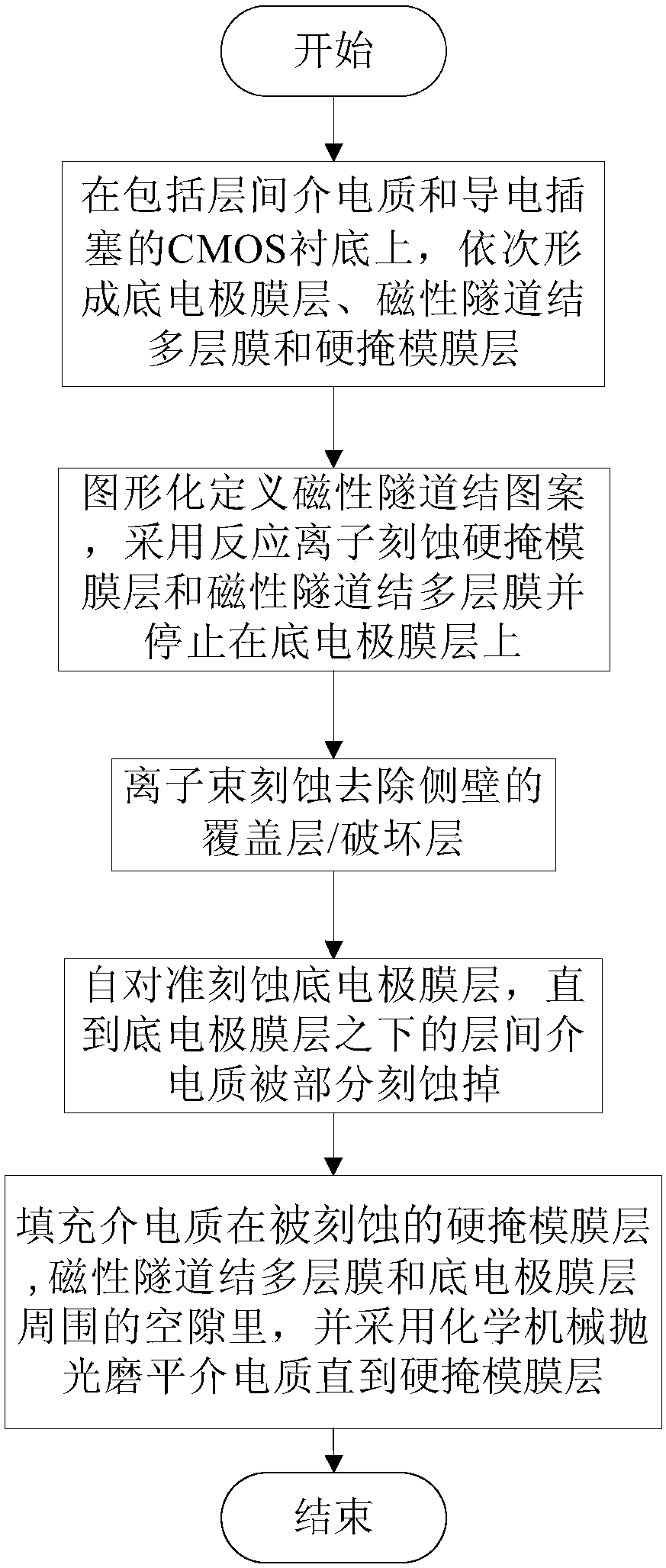
[0039] In order to make the above objects, features and advantages of the present invention more comprehensible, specific implementations of the present invention will be described in detail below in conjunction with the accompanying drawings. It should be noted that all the drawings of the present invention are in simplified form and use inaccurate scales, and are only used to facilitate and clearly assist the purpose of illustrating the embodiments of the present invention.

[0040] Such as figure 1 Shown, the present invention provides a kind of preparation method of magnetic random access memory, comprises the following steps:

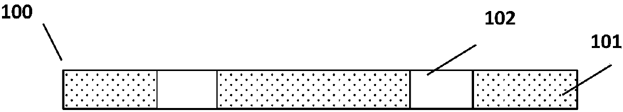
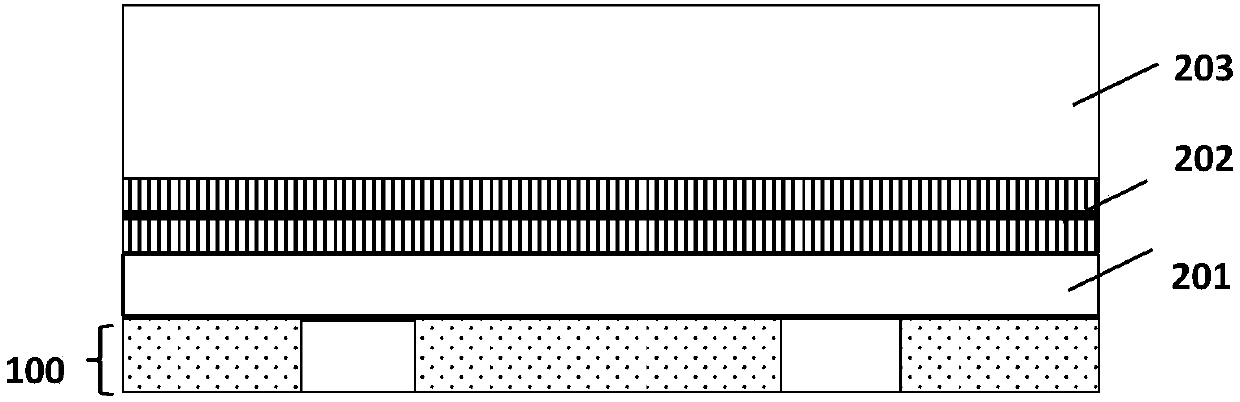
[0041] Step 1: On the CMOS substrate including the interlayer dielectric 101 and the conductive plug 102, such as figure 2 As shown, the bottom electrode film layer 201, the magnetic tunnel junction multilayer film 202 and the hard mask film layer 203 are sequentially formed, as Figure 3A shown;

[0042] Wherein, the bottom electrode film laye...


PUM

PropertyMeasurementUnit
Thicknessaaaaaaaaaa
Thicknessaaaaaaaaaa
Thicknessaaaaaaaaaa

Abstract

The invention provides a magnetic random access memory preparing method. The method comprises the steps that (1) a bottom electrode film layer, a magnetic tunnel junction multilayer film and a hard mask film layer are sequentially formed on a CMOS substrate; (2) patterning defining is carried out on a magnetic tunnel junction pattern, and the hard mask film layer and the magnetic tunnel junction multilayer film are etched and stopped on the bottom electrode film layer; (3) ion beam etching is carried out to remove the capping layer/damaging layer of a sidewall; (4) self-alignment etching is carried out on the bottom electrode film layer until an interlayer dielectric under the bottom electrode film layer is partially etched away; and (5) the dielectric is filled and ground. According to the magnetic random access memory preparing method provided by the invention, a magnetic tunnel junction is firstly prepared, and then a bottom electrode is fabricated to improve the precision of mutualalignment of the bottom electrode and the magnetic tunnel junction; and when the bottom electrode is etched, self-alignment is used without an additional bottom electrode photomask, which reduces theprocess complexity and manufacturing cost and facilitates MRAM mass production.

Description

technical field [0001] The invention relates to the technical field of integrated circuit manufacturing, in particular to a method for preparing a magnetic random access memory. Background technique [0002] In recent years, Magnetic Random Access Memory (MRAM, Magnetic Radom Access Memory), which utilizes the magnetoresistance effect of Magnetic Tunnel Junction (MTJ, Magnetic Tunnel Junction), is considered to be the future solid-state non-volatile memory, which has high-speed read-write, Features of large capacity and low energy consumption. [0003] Ferromagnetic MTJ is usually a sandwich structure, which has a magnetic memory layer, which can record different data by changing the magnetization direction; an insulating tunnel barrier layer in the middle; and a magnetic reference layer, located on the other side of the tunnel barrier layer , its magnetization direction remains unchanged. [0004] In order to record information in this magnetoresistive element, a writing ...

Claims


Application Information

Patent Timeline
IPC IPC(8): H01L27/22H01L43/12
Inventor 张云森肖荣福郭一民陈峻
Owner SHANGHAI CIYU INFORMATION TECH
Why Eureka
Try Eureka