Line-embedded flexible printed circuit and film pasting preparation technology thereof

A flexible circuit board and preparation process technology, which is applied in the secondary processing of printed circuits, coating of non-metallic protective layers, etc., can solve problems such as the inability to meet the needs of low-line spacing circuit boards, reduce the risk of short circuits, and be easy to implement and prepare. The effect of low process cost

Active Publication Date: 2018-01-23
AKM ELECTRONICS INDAL PANYU
View PDF6 Cites 2 Cited by
  • Summary
  • Abstract
  • Description
  • Claims
  • Application Information

AI Technical Summary

Problems solved by technology

The minimum pitch (the distance between the center points of two adjacent circuits) produced in the traditional subtractive process in the prior art is 60 μm, but most of the ones that can be mass-produced are 70 μm; the limit of the semi-additive process 40μm, most of which can be mass-produced are 50μm, but it still cannot meet the market's demand for low line spacing circuit boards

Method used


Image

  • Line-embedded flexible printed circuit and film pasting preparation technology thereof
  • Line-embedded flexible printed circuit and film pasting preparation technology thereof
  • Line-embedded flexible printed circuit and film pasting preparation technology thereof

Examples


Embodiment 1

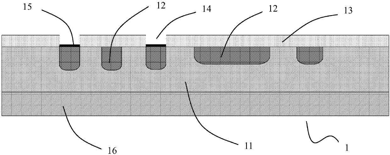
[0036] see Figure 1 to Figure 9 , a single-sided flexible circuit board 1 of this embodiment, including an adhesive layer 11, a circuit 12 embedded in the adhesive layer 11, a solder resist layer 13 located on one side of the adhesive layer 11, and a surface located on the other side of the adhesive layer 11 The protective layer 16 is provided with a plurality of pad areas 14 on the solder resist layer, the pad areas 14 are connected and penetrated with the circuit 12 , and the upper surface of the circuit 12 in the pad area 14 has a surface treatment layer 15 . In this embodiment, the material of the surface protection layer 16 is polyimide (PI), specifically thermoplastic polyimide (TPI), the material of the solder resist layer 13 is solder resist ink, and the surface treatment layer is a metal coating. From top to bottom, there are gold layer, palladium layer and nickel layer, and the thicknesses are 0.05-0.15 μm, 0.05-0.15 μm, and 3-8 μm in sequence.

[0037] This embodi...


PUM


Abstract

The invention discloses a line-embedded flexible printed circuit. The flexible printed circuit comprises a bonding layer, lines embedded into the bonding layer, a solder mask layer located on one sideof the bonding layer and a surface protection layer located on the other side of the bonding layer, the solder mask layer is provided with a plurality of pad areas which are connected and communicatewith the lines, and the upper surfaces of the lines in the pad areas are provided with surface processing layers. According to the flexible printed circuit, the lines are embedded into the bonding layer, the width and the line spacing of the lines are decreased on the premise that the high reliability is kept, the product is ultrathin and good in bendability and assemblability, and the packagingshort circuit risk of a client can be reduced. The invention further discloses a film pasting preparation technology of the flexible printed circuit. The film pasting preparation technology of the flexible printed circuit is low in cost, high in reliability, easy to achieve and capable of achieving batch production.

Description

technical field [0001] The invention belongs to the technical field of printed circuits, and in particular relates to a flexible circuit board and a film-sticking preparation process thereof. Background technique [0002] With the continuous advancement of science and technology, the consumer electronics industry such as mobile phones, Pads and other products are developing rapidly, and the demand for miniaturization and high resolution of the display screen is becoming more and more urgent, thus increasing the requirements for the fineness of the circuit of the flexible board package carrier board. Require. The minimum pitch (the distance between the center points of two adjacent circuits) produced in the traditional subtractive process in the prior art is 60 μm, but most of the mass production can be achieved with 70 μm; the semi-additive process limit 40μm, most of which can be mass-produced are 50μm, but it still cannot meet the market's demand for low-pitch circuit boa...

Claims


Application Information

Patent Timeline
Patent Type & Authority Applications(China)
IPC IPC(8): H05K3/28
Inventor 邓明黄大兴徐青松
Owner AKM ELECTRONICS INDAL PANYU
Why Eureka
Try Eureka