CMOS transconductance unit circuit with wide input voltage range and high linearity

A voltage range and high linearity technology, applied in the direction of electrical components, logic circuits, logic circuit connection/interface layout, etc., can solve the problems of small input voltage space, high power consumption and hardware cost, and reachability, and achieve wide Effects of input range, high linearity, and simple structure

Active Publication Date: 2018-02-06
SUZHOU UNIV
View PDF5 Cites 3 Cited by
  • Summary
  • Abstract
  • Description
  • Claims
  • Application Information

AI Technical Summary

Problems solved by technology

At present, the power supply voltage of the mainstream CMOS manufacturing process has dropped to 1.8V, 1.2V or even below, but the threshold voltage and drain-source saturation voltage drop cannot be reduced in the same proportion, so the space left for the input voltage is getting smaller and smaller.
In fact, the maximum value of the common-mode input voltage cannot reach the value of VDD-Vdsat4-Vgs1, because when the drain-source voltage of M4 is close to Vdsat4, the output transconductance of the M4 tube begins to increase, resulting in the M2 tube-M3 tube Current mirrored to output increases
The equivalent transconductance at this time increases, but it is no longer mainly determined by the passive resistance, so the linearity of the transconductance deteriorates
[0004] It is true that a linear transconductance unit with a large input range can be realized by using a rail-to-rail operational amplifier, etc., but the power consumption and hardware cost are very high, which does not meet the requirements of the increasingly complex and large system-on-chip for low power consumption and compact area of ​​the basic module.

Method used


Image

  • CMOS transconductance unit circuit with wide input voltage range and high linearity
  • CMOS transconductance unit circuit with wide input voltage range and high linearity
  • CMOS transconductance unit circuit with wide input voltage range and high linearity

Examples


Embodiment 1

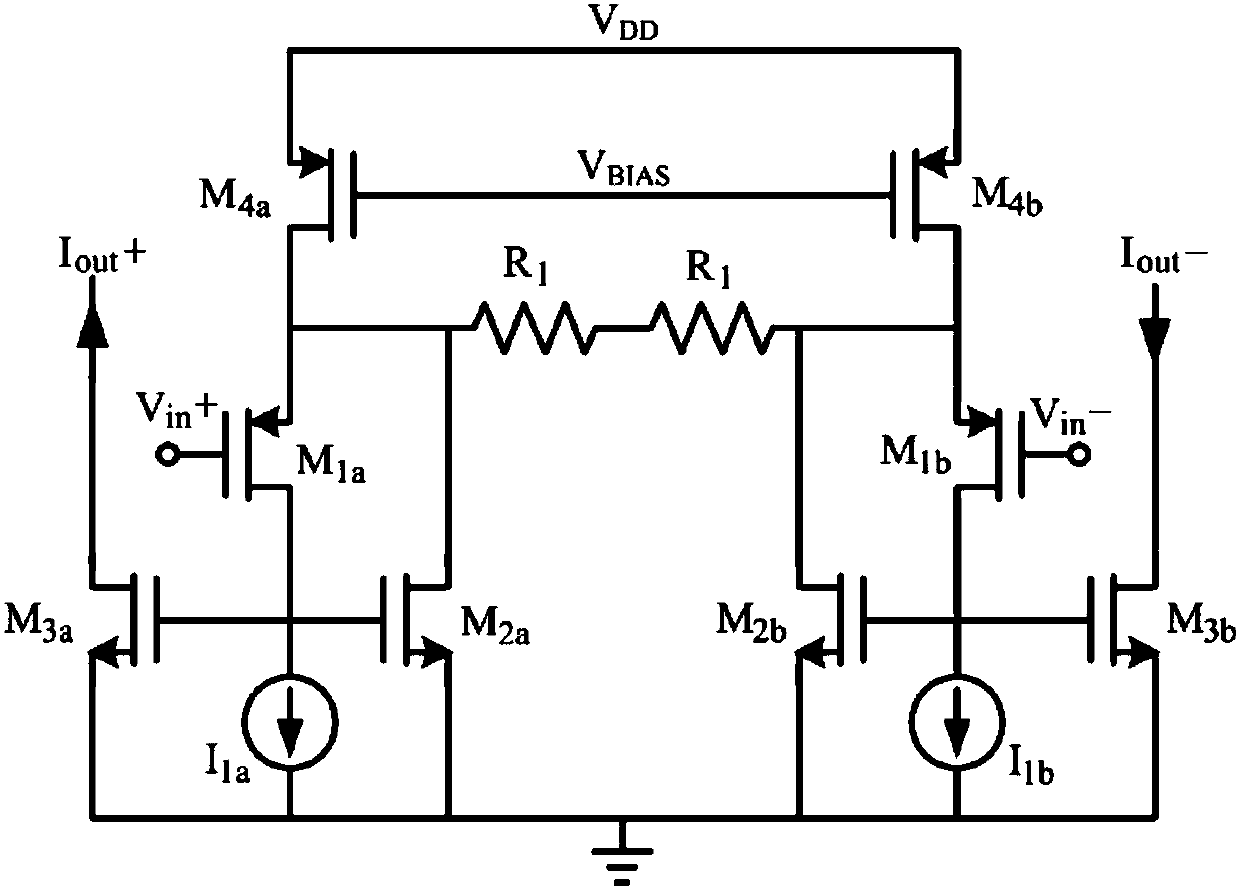
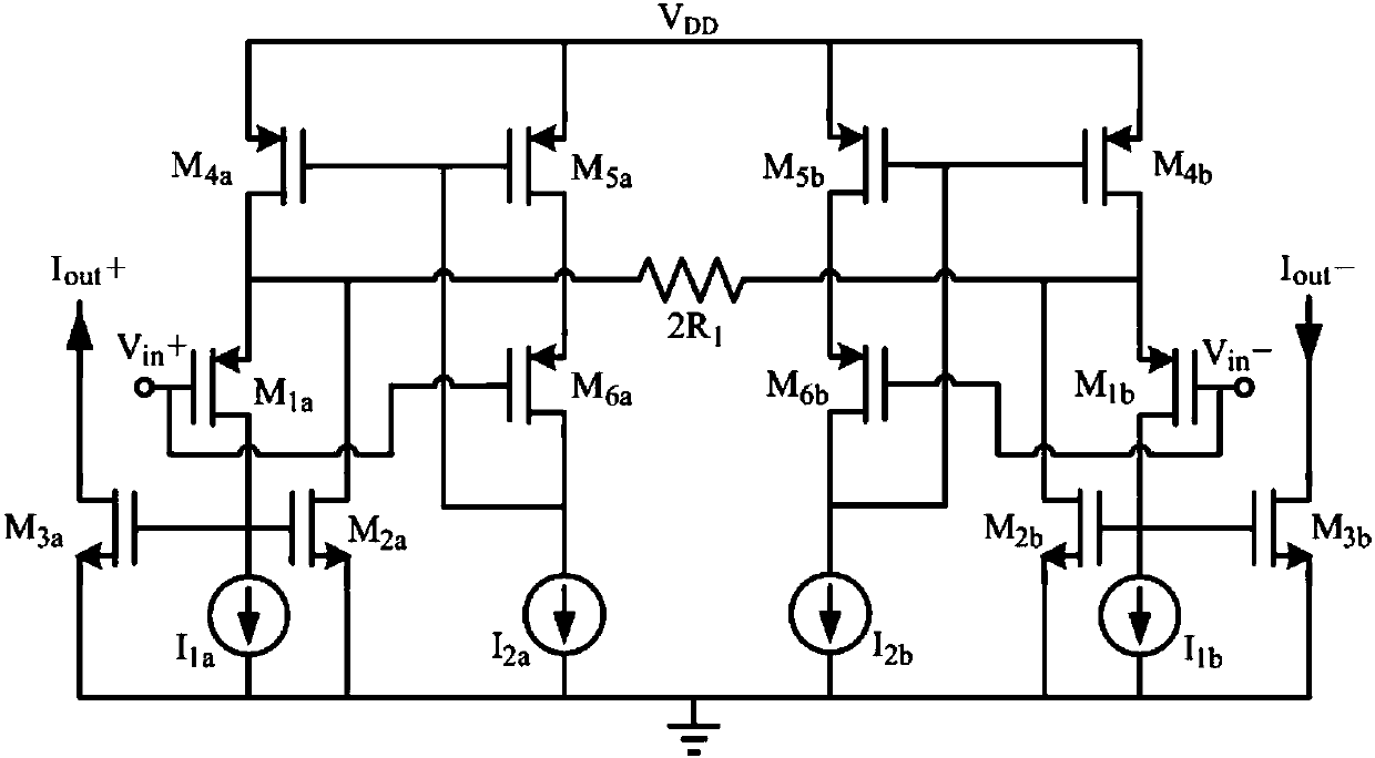
[0027] see figure 2 As shown, a wide input voltage range high linearity CMOS transconductance unit circuit, which includes a bias constant current source, a differential input stage, and an output current mirror,

[0028] The bias constant current source includes a first PMOS transistor M4a, a second PMOS transistor M5a matching the first PMOS transistor M4a, a third PMOS transistor M5b and a fourth PMOS transistor M4b matching the third PMOS transistor M5b, the The sources of the first PMOS transistor M4a, the second PMOS transistor M5a, the third PMOS transistor M5b and the fourth PMOS transistor M4b are connected to the power supply VDD, and the gate of the first PMOS transistor M4a is connected to the gate of the second PMOS transistor M5a and are commonly connected to the output terminal of the first current source I2a, the gate of the third PMOS transistor M5b is connected to the gate of the fourth PMOS transistor M4b and are commonly connected to the output terminal of...


PUM


Abstract

The invention discloses a CMOS transconductance unit circuit with the wide input voltage range and the high linearity. The circuit comprises a bias constant current source, a difference input grade and an output current mirror. The bias constant current source comprises a first PMOS tube M4a, a second PMOS tube M5a matching the first PMOS tube M4a, a third PMOS tube M5b and a fourth PMOS tube M4bmatching the third PMOS tube M5b. The difference input grade comprises a fifth PMOS tube M1a, a sixth PMOS tube M6a matching the fifth PMOS tube M1a, a seventh PMOS tube M6a and an eighth PMOS tube M1b matching the seventh PMOS tube M6a. The output current mirror comprises a first current mirror and a second current mirror, wherein the first current mirror is symmetrical to the second current mirror in a mirrored manner. The first current mirror comprises a first NMOS tube M3a and a second NMOS tube M2a. The second current mirror comprises a third first NMOS tube M2b and a fourth NMOS tube M3b. According to the invention, the circuit is characterized by wide common-mode input range and high linearity; the transconductance value can be tuned; and the circuit can be used for achieving high-linearity amplifier with variable gain and a tunable Gm-C integrator.

Description

technical field [0001] The invention relates to the field of analog integrated circuit design, in particular to a CMOS transconductance unit circuit with wide input voltage range and high linearity. Background technique [0002] With the rapid progress of CMOS manufacturing technology, the feature size of the device is continuously reduced, and the power supply voltage is also continuously reduced, resulting in the limitation of the common-mode input voltage range of the transconductance unit implemented by the classic differential pair. Usually we introduce source degeneration resistors into the differential pair structure to improve the linearity of the transconductance unit. On this basis, we can enhance the transconductance of the input MOS pair tube and increase the degeneration depth, which can further improve the linearity of the transconductance unit, but It also faces the problem of limited common-mode input voltage range. [0003] see figure 1 As shown, it is a t...

Claims


Application Information

Patent Timeline
Patent Type & Authority Applications(China)
IPC IPC(8): H03K19/0185
CPCH03K19/018521
Inventor 白春风王洋
Owner SUZHOU UNIV
Why Eureka
Try Eureka