Circuit board structure

A technology for circuit boards and patterned circuit layers, applied in printed circuits, printed circuits, printed circuit manufacturing, etc., can solve problems affecting process yield and complicated steps, so as to improve production process efficiency, improve yield, and simplify process The effect of steps

Pending Publication Date: 2018-02-06
同扬光电(江苏)有限公司
View PDF5 Cites 2 Cited by
  • Summary
  • Abstract
  • Description
  • Claims
  • Application Information

AI Technical Summary

Problems solved by technology

[0004] It is worth noting that during the above-mentioned laser drilling process, the smear that has not been completely removed by the laser will remain on the hole wall of the blind hole, so it is still necessary to remove the smear with an alkaline chemical solution. Therefore, currently The blind hole process steps are still quite complicated
Moreover, in the process of desmearing, the copper layer under the blind hole is easy to peel off in the alkaline chemical solution, thus affecting the yield of the process

Method used


Image

  • Circuit board structure
  • Circuit board structure
  • Circuit board structure

Examples


Embodiment Construction

[0044] The aforementioned and other technical contents, features and effects of the present invention will be clearly presented in the following detailed descriptions of the embodiments with accompanying drawings. The directional terms mentioned in the following embodiments, such as "upper", "lower", "front", "rear", "left", "right", etc., are only referring to the directions of the drawings. Accordingly, the directional terms used are intended to illustrate rather than limit the present invention. Also, in the following embodiments, the same or similar components will use the same or similar symbols.

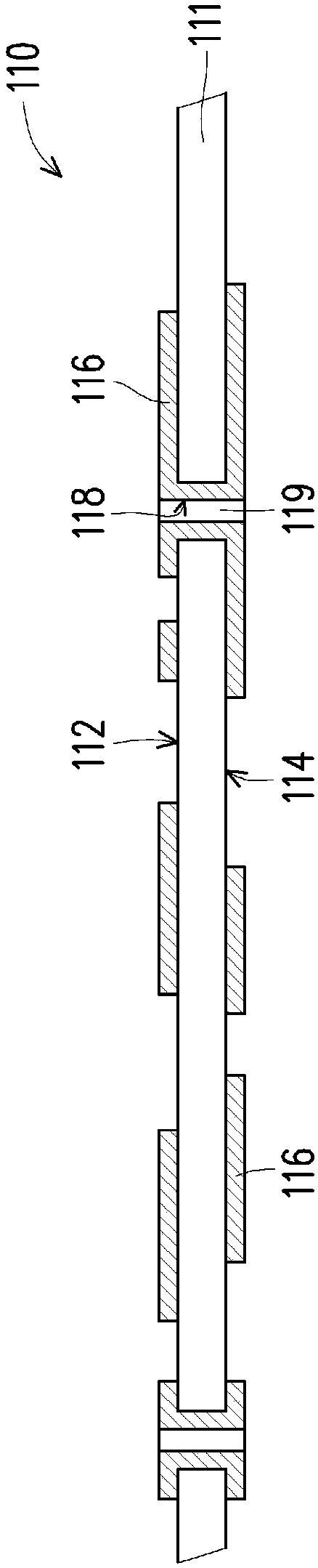
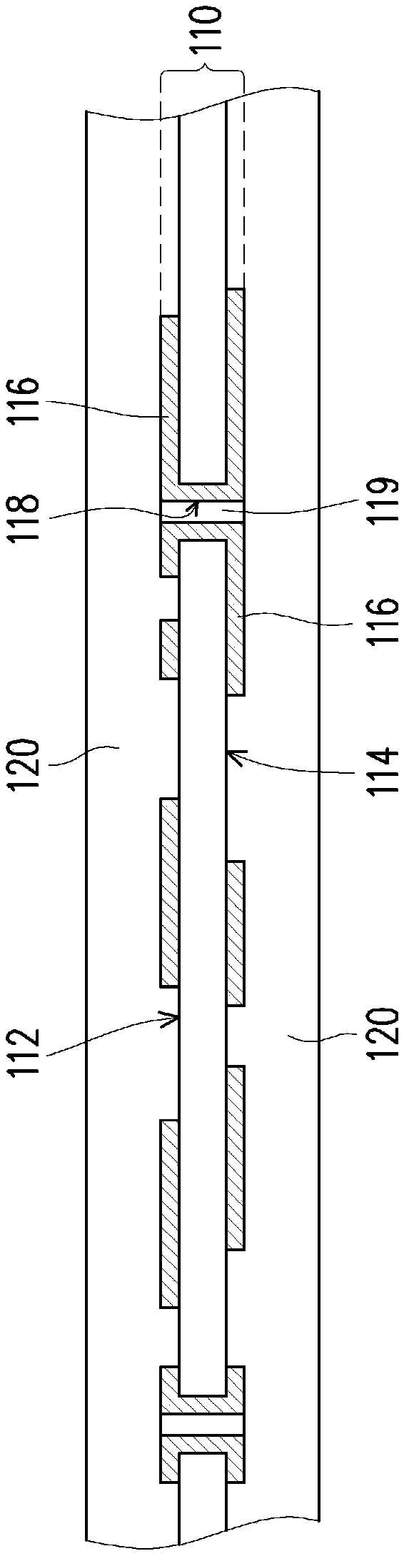
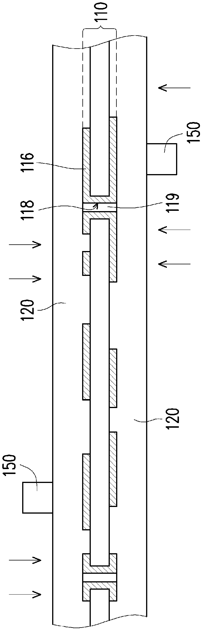
[0045] Figure 1A to Figure 1I It is a schematic cross-sectional flow diagram of a manufacturing method of a circuit board structure according to an embodiment of the present invention. The manufacturing method of the circuit board structure in this embodiment includes the following steps. First, provide the Figure 1A The substrate 110 is shown, wherein the substrate 110 in...


PUM


Abstract

The present invention provides a circuit board structure. The circuit board structure comprises a base plate, a plurality of metallizable photosensitive developing substrates, an electroless plated seed layer, and a second patterned circuit layer; the substrate includes an upper surface, a lower surface opposite to the upper surface, and a first patterned circuit layer; the metallizable photosensitive developing substrates are respectively disposed on the upper surface and the lower surface; each of the metallizable photosensitive development substrate includes a plurality of blind holes whichexpose at least a portion of the first patterned wiring layer; the materials of the metallizable photosensitive development substrates contain a photosensitive material; the electroless plated seed layer is disposed on the metallizable photosensitive substrates and covers the inner walls of the blind holes; and the second patterned circuit layer is disposed on the first electroless plated seed layer and fills the blind holes so as to be electrically connected with the first patterned circuit layer. According to the circuit board structure, the process steps of the circuit board structure areeffectively simplified, and the process efficiency of the circuit board structure is improved.

Description

technical field [0001] The invention relates to a circuit board structure, in particular to a circuit board structure with a metallizable photosensitive and developable base material. Background technique [0002] In the current semiconductor packaging manufacturing process, the circuit board has become one of the frequently used structural components due to the advantages of fine wiring, compact assembly and good performance. The circuit board can be assembled with a plurality of electronic components, such as chips and passive components. Through the circuit board, these electronic components are electrically connected to each other, and signals can be transmitted between these electronic components. [0003] Generally speaking, a circuit board is mainly composed of multiple patterned circuit layers and multiple insulating layers laminated alternately, and the patterned circuit layers are electrically connected to each other through conductive vias. The traditional metho...

Claims


Application Information

Patent Timeline
Patent Type & Authority Applications(China)
IPC IPC(8): H05K1/11H05K3/42H05K3/46
CPCH05K1/115H05K3/429H05K3/4644H05K2201/09509H05K2203/0723H05K2203/072
Inventor 刘逸群段嵩庆洪培豪沈建成李远智
Owner 同扬光电(江苏)有限公司
Why Eureka
Try Eureka