Detection method for cross effects of array substrate

A technology of an array substrate and a detection method, which is applied in the field of detection of reticle defects of array substrates, can solve problems such as G/D coordinate errors, reticle defects, and high requirements for machine positioning accuracy, so as to reduce production costs and improve factory efficiency. , The effect of improving product yield

Active Publication Date: 2018-02-09
TCL CHINA STAR OPTOELECTRONICS TECH CO LTD
View PDF4 Cites 6 Cited by
  • Summary
  • Abstract
  • Description
  • Claims
  • Application Information

AI Technical Summary

Problems solved by technology

[0005] Among them, the front-end array manufacturing process specifically includes: forming horizontal wires (including scanning lines and common electrode lines), vertical wires (including data lines), TFTs electrically connected with horizontal wires and vertical wires, and transparent wires on a transparent substrate. electrodes and other structures to produce an array substrate, in which the horizontal wires and vertical wires are respectively formed in the two metal layers of the insulating layer. Since the manufacturing process is prone to short circuits at the crossing positions of the horizontal wires and vertical wires, forming cross-line defects, so in After the array substrate is manufactured, array testing is required to find out the specific position of the cross-hair defect, which can be repaired by the subsequent repair site according to the specific position of the cross-hair defect. In the prio

Method used


Image

  • Detection method for cross effects of array substrate
  • Detection method for cross effects of array substrate
  • Detection method for cross effects of array substrate

Examples


Embodiment Construction

[0033] In order to further illustrate the technical means adopted by the present invention and its effects, the following describes in detail in conjunction with preferred embodiments of the present invention and accompanying drawings.

[0034] see Figure 4 , the present invention provides a method for detecting crosshair defects on an array substrate, comprising the following steps:

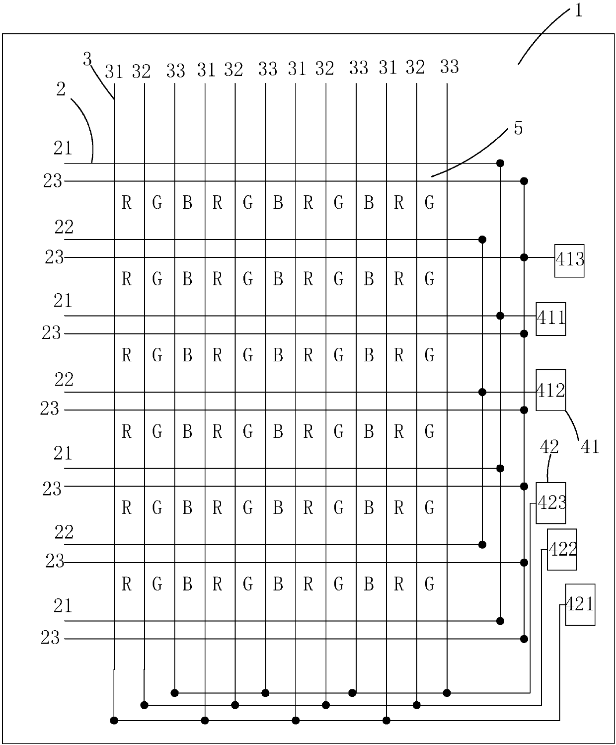
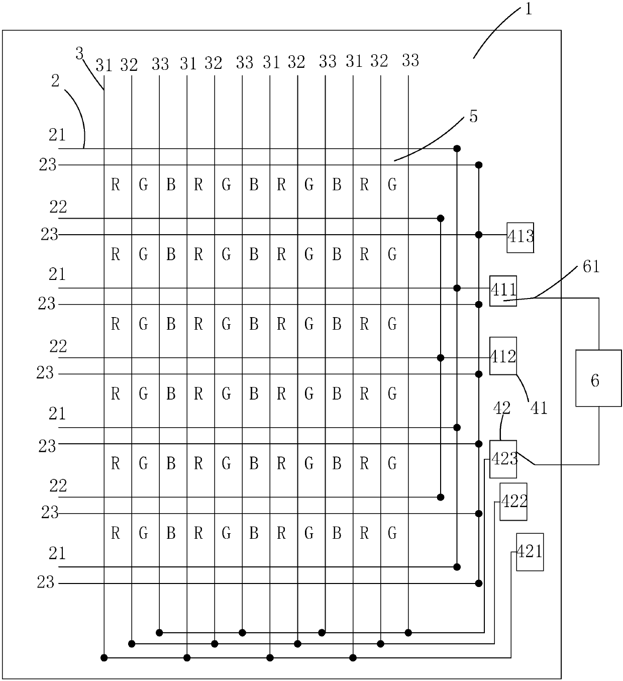
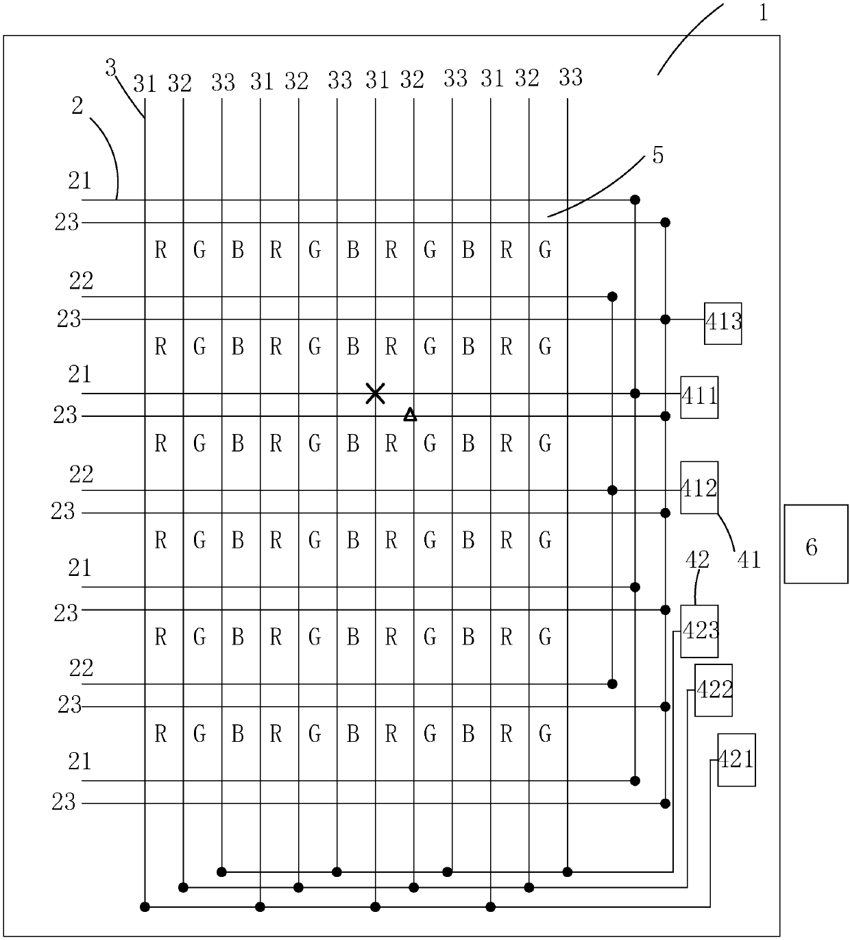
[0035] Step 1. Please refer to figure 1 , providing an array substrate, including: a substrate 1, a plurality of horizontal scan lines 2 arranged in parallel and spaced along the vertical direction arranged on the substrate 1, a plurality of horizontal scan lines 2 arranged in parallel and spaced in a vertical direction arranged on the substrate 1 Conductive wires 2 , and multiple rows of vertical conductive wires 3 arranged in parallel and spaced apart on the substrate 1 .

[0036] Specifically, in a preferred embodiment of the present invention, the array substrate adopts 2G3D technology, a...


PUM


Abstract

The invention provides a detection method for cross effects of an array substrate. The method comprises the steps: classifying horizontal wires and vertical wires; enabling the horizontal wires of thesame type to be electrically connected to the same horizontal wire bonding pad; enabling the vertical wires of the same type to be electrically connected with the same vertical wire bonding pad; measuring the resistance values between each vertical wire bonding pad and all horizontal wire bonding pads; recording the vertical wire bonding pad and the horizontal wire bonding pad corresponding to anabnormal resistance value; calculating and obtaining the horizontal wire and the vertical wire, which are the nearest to right-angle coordinates and are respectively electrically connected with the vertical wire bonding pad and the horizontal wire bonding pad corresponding to the abnormal resistance value, according to the detected right-angle coordinates, thereby determining the position of cross defects. Compared with the prior art, the method can accurately obtain the position of the cross defects of the array substrate through electrical testing equipment with the lower precision, improves the yield, reduces the production cost, and improves the benefits of a factory.

Description

technical field [0001] The invention relates to the field of display technology, in particular to a method for detecting crosshair defects on an array substrate. Background technique [0002] With the development of display technology, liquid crystal displays (Liquid Crystal Display, LCD) and other flat display devices are widely used in mobile phones, televisions, personal Various consumer electronic products such as digital assistants, digital cameras, notebook computers, and desktop computers have become the mainstream of display devices. [0003] Most of the liquid crystal display devices currently on the market are backlight liquid crystal displays, which include a liquid crystal display panel and a backlight module. The working principle of the liquid crystal display panel is to place liquid crystal molecules between two parallel glass substrates. There are many vertical and horizontal small wires between the two glass substrates. The direction of the liquid crystal m...

Claims


Application Information

Patent Timeline
IPC IPC(8): G09G3/00
CPCG09G3/006
Inventor 肖平坦
Owner TCL CHINA STAR OPTOELECTRONICS TECH CO LTD
Why Eureka
Try Eureka