Supercharge Your Innovation With Domain-Expert AI Agents!

Highly efficient and easy-to-use field-effect transistor (FET)

A field effect tube, high-efficiency technology, applied in the direction of electrical components, electric solid devices, circuits, etc., can solve the problems that affect the normal use of field effect tubes, cannot quickly find field effect tubes, and field effect tubes are scrapped

Inactive Publication Date: 2018-02-16
长兴三通能源科技有限公司
View PDF1 Cites 0 Cited by
  • Summary
  • Abstract
  • Description
  • Claims
  • Application Information

AI Technical Summary

Problems solved by technology

[0004] The purpose of the present invention is to provide a highly efficient and easy-to-use field effect transistor to solve the problem that the drain, gate and source are exposed to the air for a long time when they are idle, which is prone to oxidation and affects the field effect. The normal use of the tube, and when the drain, gate and source are damaged, they cannot be replaced individually, resulting in the scrapping of the entire field effect tube, and the problem of the field effect tube cannot be quickly found when the ring mirror is dark

Method used


Image

  • Highly efficient and easy-to-use field-effect transistor (FET)
  • Highly efficient and easy-to-use field-effect transistor (FET)
  • Highly efficient and easy-to-use field-effect transistor (FET)

Examples


Embodiment 1

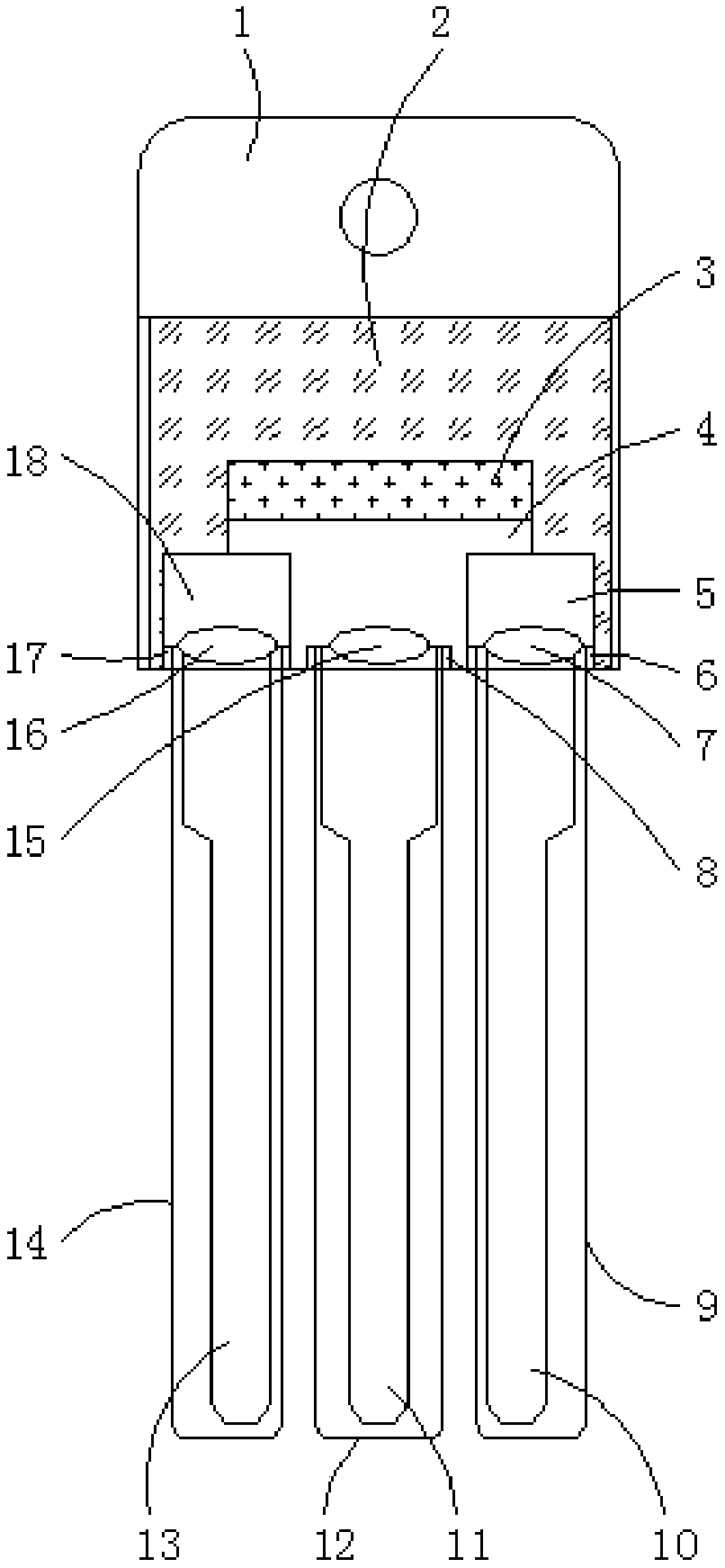
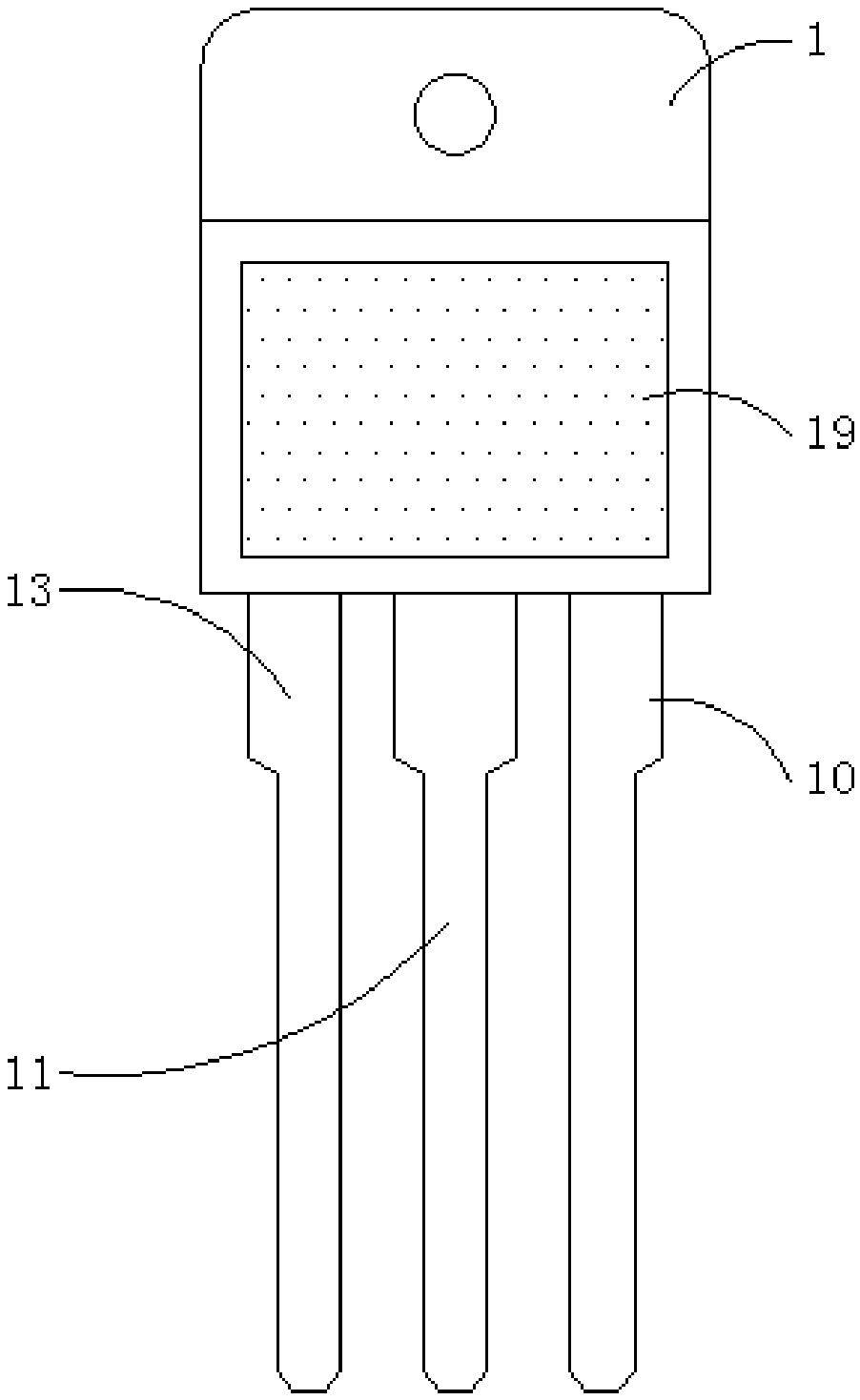
[0023] see Figure 1-3 , the present invention provides a technical solution: a highly efficient and easy-to-use field effect tube, including a field effect tube outer shell 1, a fluorescent plate 19 is embedded on the front surface wall of the field effect tube shell 1, and the field effect A P-type semiconductor 2 , an oxide 3 , a metal 4 , a first N-type semiconductor 5 , and a second N-type semiconductor 18 are arranged inside the tube shell 1 .

[0024] Further, the oxide 3 and the metal 4 are embedded in the P-type semiconductor 2, the metal 4 is installed under the oxide 3, and the first N-type semiconductor 5 and the second N-type semiconductor 18 are embedded in the metal 4. , and the first N-type semiconductor 5 and the gate groove 8 both extend from the inside of the metal 4 to the inside of the P-type semiconductor 2, so that the field effect transistor can function as an amplifying circuit and changing resistance.

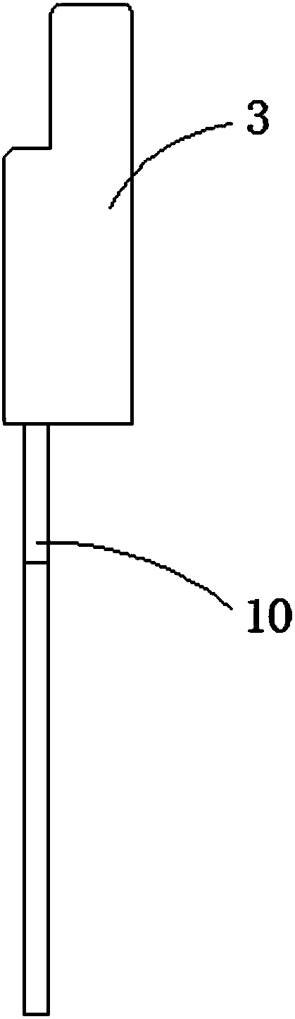
[0025] Specifically, a drain groove 17 is opene...

Embodiment 2

[0030] Figure 4 It is a structural schematic diagram of Embodiment 2 of an efficient protection and easy-to-use field effect tube of the present invention; as Figure 4 As shown, the parts that are the same as or corresponding to those in Embodiment 1 use the reference numerals corresponding to Embodiment 1. For the sake of simplicity, only the differences from Embodiment 1 will be described below. The difference between this embodiment two and embodiment one is:

[0031] Such as Figure 4As shown, a field effect transistor with high efficiency protection and easy to use, when in use, the drain bellows 14, the gate bellows 12 and the source bellows 9 can also be separated from the drain groove 17, the gate Tear off the groove 8 and the source groove 6, and fall off from top to bottom along the drain 13, the gate 11 and the source 10 respectively, so that the drain 13, the gate 11 and the source 10 are exposed, and then Insert the drain 13 , the gate 11 and the source 10 in...


PUM


Abstract

The invention discloses a highly efficient and easy-to-use field-effect transistor (FET), which comprises a FET outer shell. A fluorescent plate is embedded in the front wall of the FET outer shell, and a P-type semiconductor, an oxide, metal, a first N-type semiconductor and a second N-type semiconductor are arranged inside the FET outer shell. In the invention, a drain welding point is welded inside a drain groove, a gate welding point is welded inside the metal, a source welding point is welded inside the first N-Type semiconductor, a drain, a gate and a source can be respectively welded into the drain groove, a gate groove and a source groove through the drain welding point, the gate welding point and the source welding point, when the drain, the gate and the source are oxidatively corroded and cannot be used normally, the corresponding welding points can be melt through a welding gun, the oxidatively corroded pins are replaced, and the problem of the traditional one-piece structure that oxidative corrosion of any pin of the drain, the gate and the source will lead to the scrapping of the entire FET is avoided.

Description

technical field [0001] The invention belongs to the technical field of electronic components, and in particular relates to an efficient protection and easy-to-use field effect tube. Background technique [0002] The working principle of field effect transistors is to put it in one sentence, that is, "the ID flowing through the channel between the drain and the source is used to control the ID of the reverse-biased gate voltage formed by the pn junction between the gate and the channel", more correctly Said, the width of the ID flowing through the channel, that is, the cross-sectional area of ​​the channel, is controlled by the change of the reverse bias of the pn junction, resulting in the change of the expansion of the depletion layer. In the unsaturated region of VGS=0, the expansion of the transition layer is represented Because it is not very large, according to the electric field of VDS applied between the drain and the source, some electrons in the source region are pu...

Claims


Application Information

Patent Timeline
IPC IPC(8): H01L23/488H01L23/06H01L23/02H01L29/772
CPCH01L23/02H01L23/06H01L23/48H01L29/772
Inventor 刘玉民
Owner 长兴三通能源科技有限公司
Features
  • R&D
  • Intellectual Property
  • Life Sciences
  • Materials
  • Tech Scout
  • Unparalleled Data Quality
  • Higher Quality Content
  • 60% Fewer Hallucinations
Learn More