Differential amplifier

A differential amplifier and differential input technology, which is applied in the direction of differential amplifiers, amplifiers, radio frequency amplifiers, etc., can solve the problems of low operating frequency, low power amplifier efficiency, and large space occupation, so as to increase the operating frequency, reduce the area, and reduce the occupation. area effect

Inactive Publication Date: 2018-02-27
UNIV OF ELECTRONICS SCI & TECH OF CHINA
View PDF4 Cites 2 Cited by
  • Summary
  • Abstract
  • Description
  • Claims
  • Application Information

AI Technical Summary

Problems solved by technology

[0003] However, the existing differential amplifiers based on GaN devices still have shortcomings such as large space occupation, high loss, low operating frequency, and low power amplifier efficiency.

Method used


Image

  • Differential amplifier
  • Differential amplifier
  • Differential amplifier

Examples


Embodiment Construction

[0032] The following will clearly and completely describe the technical solutions in the embodiments of the present invention with reference to the accompanying drawings in the embodiments of the present invention. Obviously, the described embodiments are only some, not all, embodiments of the present invention. Based on the embodiments of the present invention, all other embodiments obtained by persons of ordinary skill in the art without making creative efforts belong to the protection scope of the present invention.

[0033] The object of the present invention is to provide a differential amplifier.

[0034] In order to make the above objects, features and advantages of the present invention more comprehensible, the present invention will be further described in detail below in conjunction with the accompanying drawings and specific embodiments.

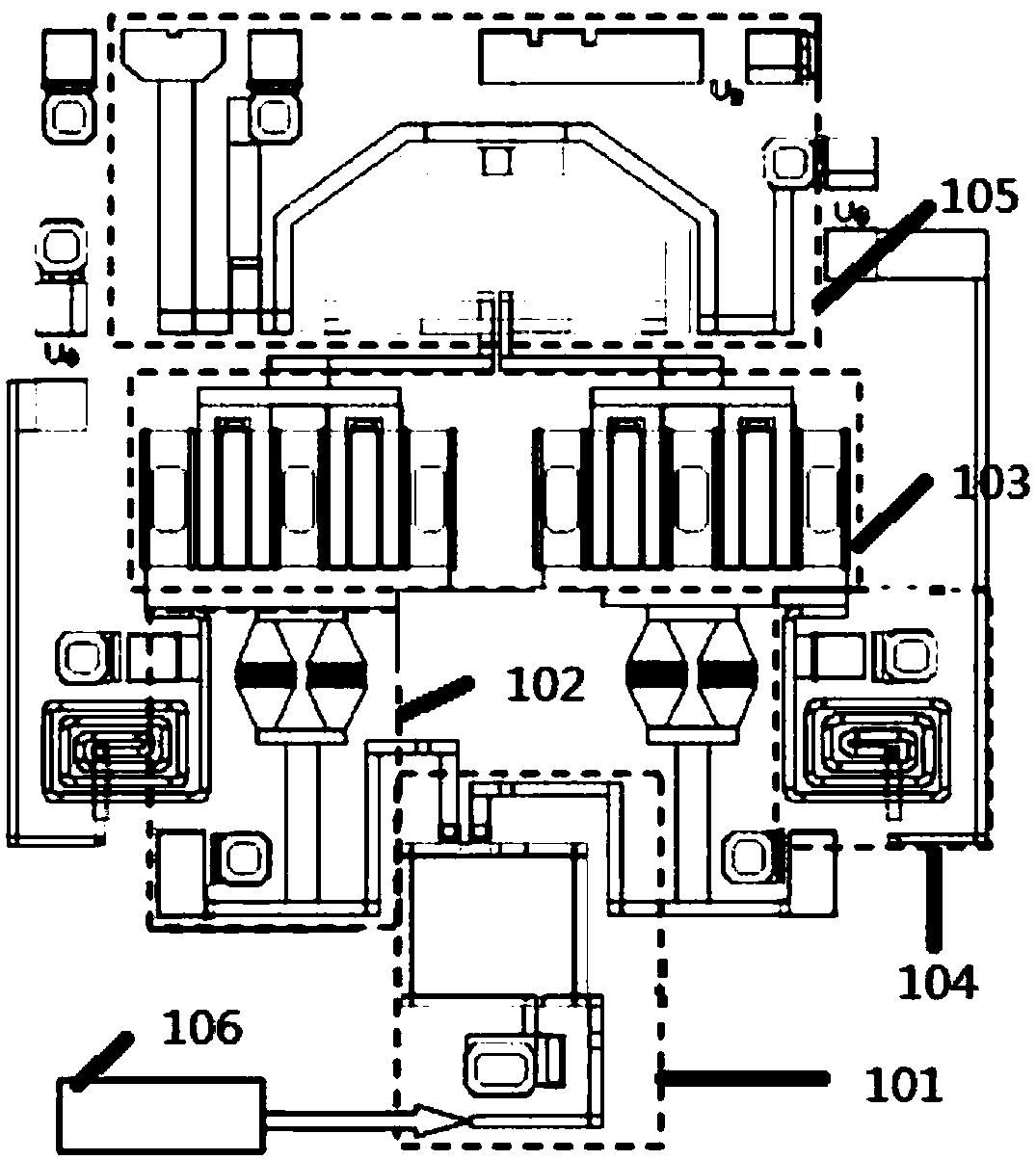
[0035] figure 1 It is a differential amplifier layout of an embodiment of a differential amplifier in this application.

[00...


PUM


Abstract

A differential amplifier, comprising a previous-stage drive level (106), an input balun (101), a matching network (102), a differential transistor pair (103), a bias network (104) and an output balun(105). An output end of the previous-stage drive level (106) is connected to an input end (203) of the input balun (101). An output end (205) of the input balun (101) is connected to an input end of the matching network (102), an output end of the matching network (102) is connected to an input end of the differential transistor pair (103) and the bias network (104), and an output end of the differential transistor pair (103) is connected to the output balun (105). The input balun (101) is a single-turn stacked transformer. The output balun (105) is a planar transformer with a full inner-frameand a half outer-frame. The input balun of the differential amplifier is a single-turn stacked transformer, and the output balun has a structure with a full inner-frame and a half outer-frame, so that the differential amplifier takes up less space, and has low loss, high operating frequency and better power amplifier efficiency.

Description

technical field [0001] The invention relates to the technical field of amplifiers, in particular to a differential amplifier. Background technique [0002] Differential amplifiers are used in silicon (Si)-based circuits, such as complementary metal oxide semiconductor field effect transistors (Complementary MetalOxide Semiconductor, CMOS), because of their many advantages such as suppressing common-mode signals, reducing even-order harmonic components, and suppressing odd-mode oscillations. a wide range of applications. As a representative of the third-generation semiconductor, gallium nitride (GaN) devices have the advantages of high voltage, high frequency, and high power density. Therefore, differential amplifiers based on GaN devices can break through the limitations of power output in silicon-based circuits. [0003] However, the existing differential amplifiers based on GaN devices still have disadvantages such as large space occupation, high loss, low operating frequ...

Claims


Application Information

Patent Timeline
Patent Type & Authority Applications(China)
IPC IPC(8): H03F1/56H03F3/45
CPCH03F1/565H03F3/45179H03F2203/45624H03F2203/45031H03F2203/45148H03F3/195H03F3/45381H03F2200/451H03F2200/06H03F2200/09H01L23/00H03F3/45076
Inventor 徐跃杭肖玮刘宪锁孙博文
Owner UNIV OF ELECTRONICS SCI & TECH OF CHINA
Why Eureka
Try Eureka