A method for preparing β-gallium oxide thin film on silicon substrate

A gallium oxide, silicon substrate technology, applied in semiconductor/solid-state device manufacturing, electrical components, circuits, etc., can solve problems such as easy cracks and poor film quality, and achieve the effects of eliminating cracks, low cost, and simple process methods

Active Publication Date: 2019-08-02
HARBIN INST OF TECH
View PDF5 Cites 0 Cited by
  • Summary
  • Abstract
  • Description
  • Claims
  • Application Information

AI Technical Summary

Problems solved by technology

[0006] The purpose of the present invention is to provide a method for preparing a β-gallium oxide film on a silicon substrate in order to solve the problems of poor film quality and cracks caused by large lattice mismatch and thermal mismatch. The method first prepares β-Ga 2 o 3 nanopillar arrays as a buffer layer, and then the β-Ga 2 o 3 Preparation of β-Ga on Nanopillar Arrays 2 o 3 film

Method used


Image

  • A method for preparing β-gallium oxide thin film on silicon substrate

Examples


specific Embodiment approach 1

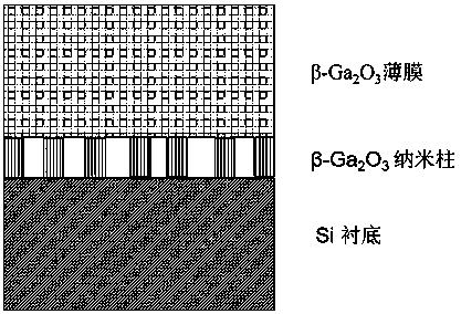
[0022] Specific implementation mode 1: This implementation mode records a method for preparing a β-gallium oxide thin film on a silicon substrate, and the steps of the method are as follows:

[0023] Step 1: Prepare GaOOH seed layer by water bath method;

[0024] Get a silicon substrate, and it is cleaned, stand-by; Water bath method configures gallium nitrate (Ga(NO 3 ) 3 ) and hexamethylenetetramine (HMT) mixed solution, and the growth surface of the substrate used is placed in the mixed solution for growth; wherein, the concentration of gallium nitrate is 0.1~0.6mol / L, and the concentration of hexamethylenetetramine is 0.5~1mol / L, the total volume of the mixed solution is 30 mL, the temperature of the water bath is 80-98 o C, the growth time is 1-3h;

[0025] Step 2: After washing the substrate with the seed layer obtained in Step 1 with deionized water, put it into an oven at 150 o Dry at C temperature, then put it into the hydrothermal mixed solution to react, after t...

Embodiment 1

[0033] A method for preparing a β-gallium oxide thin film on a silicon substrate, the steps of the method are as follows:

[0034] Step 1: Prepare GaOOH seed layer by water bath method;

[0035] Get a silicon substrate, and it is cleaned, stand-by; Water bath method configures gallium nitrate (Ga(NO 3 ) 3 ) and hexamethylenetetramine (HMT) mixed solution, place the substrate growth side down in the mixed solution for growth; wherein, the concentration of gallium nitrate is 0.5mol / L, and the concentration of hexamethylenetetramine is 0.5mol / L, the total volume of the mixed solution is 30 mL, and the temperature of the water bath is 90 o C, the growth time is 3h;

[0036] Step 2: After washing the substrate with the seed layer obtained in Step 1 with deionized water, put it into an oven at 150 o Dry at C temperature, then put it into the hydrothermal mixed solution to react, after the reaction, cool down naturally, take out the substrate, wash it with deionized water, and p...


PUM


Abstract

The invention relates to a method for preparing a beta-gallium oxide thin film on a silicon substrate, and belongs to the technical field of gallium oxide thin film preparation. The method comprises the following steps of 1, growing a beta-gallium oxide nano-rod array on a silicon substrate as a buffer layer; 2, preparing a beta-gallium oxide thin film on the beta-gallium oxide nano-rod array served as the buffer layer. According to the invention, a beta-Ga2O3 nano-rod buffer layer is inserted between a silicon substrate and an epitaxial layer. The lattices of the beta-Ga2O3 nano-rod buffer layer are the same as the lattices of the epitaxial layer, so that the lattice mismatch can be reduced. Meanwhile, the thermal stress caused by the stress and the huge difference between thermal expansion coefficients during the growth process can be transferred and released due to the existence of gaps among nano-rods. Cracks caused by thermal mismatch in the annealing process are eliminated. Therefore, a large-area, uniform and high-quality beta-Ga2O3 thin film is obtained. Meanwhile, the method is simple in process, low in cost and great in application potential.

Description

technical field [0001] The invention belongs to the technical field of semiconductor material preparation, and in particular relates to a method for preparing a β-gallium oxide thin film on a silicon substrate. Background technique [0002] At present, β-gallium oxide (β-Ga 2 o 3 ) film quality is poor, and due to lattice mismatch and thermal mismatch in the high-temperature annealing process, the crystal quality decreases, and even cracks occur, which is difficult to meet the requirements of optoelectronic device applications, thus limiting the application of β-gallium oxide films . [0003] Gallium oxide thin films have various crystal phases such as α, β, γ, etc., among which only β-Ga 2 o 3 In order to stabilize the crystal phase, other crystal phases can be transformed into β-Ga at high temperature 2 o 3 , β-Ga 2 o 3 It is a wide bandgap semiconductor with a bandgap of 4.9 eV, which is much larger than that of gallium nitride and silicon carbide; the electron co...

Claims


Application Information

Patent Timeline
Patent Type & Authority Patents(China)
IPC IPC(8): H01L21/02
CPCH01L21/02381H01L21/02483H01L21/02513H01L21/02565H01L21/02631
Inventor 矫淑杰张峻华李少方
Owner HARBIN INST OF TECH
Why Eureka
Try Eureka