LED packaging method
A technology of LED packaging and LED chips, which is applied in the direction of semiconductor devices, electrical components, circuits, etc., can solve the problems of reduced light intensity, insufficient concentration of light source illumination, spectral shift, etc., to reduce production costs, suppress total reflection effect, Effect of improving luminous efficiency
- Summary
- Abstract
- Description
- Claims
- Application Information
AI Technical Summary
Problems solved by technology
Method used
Image
Examples
Embodiment 1
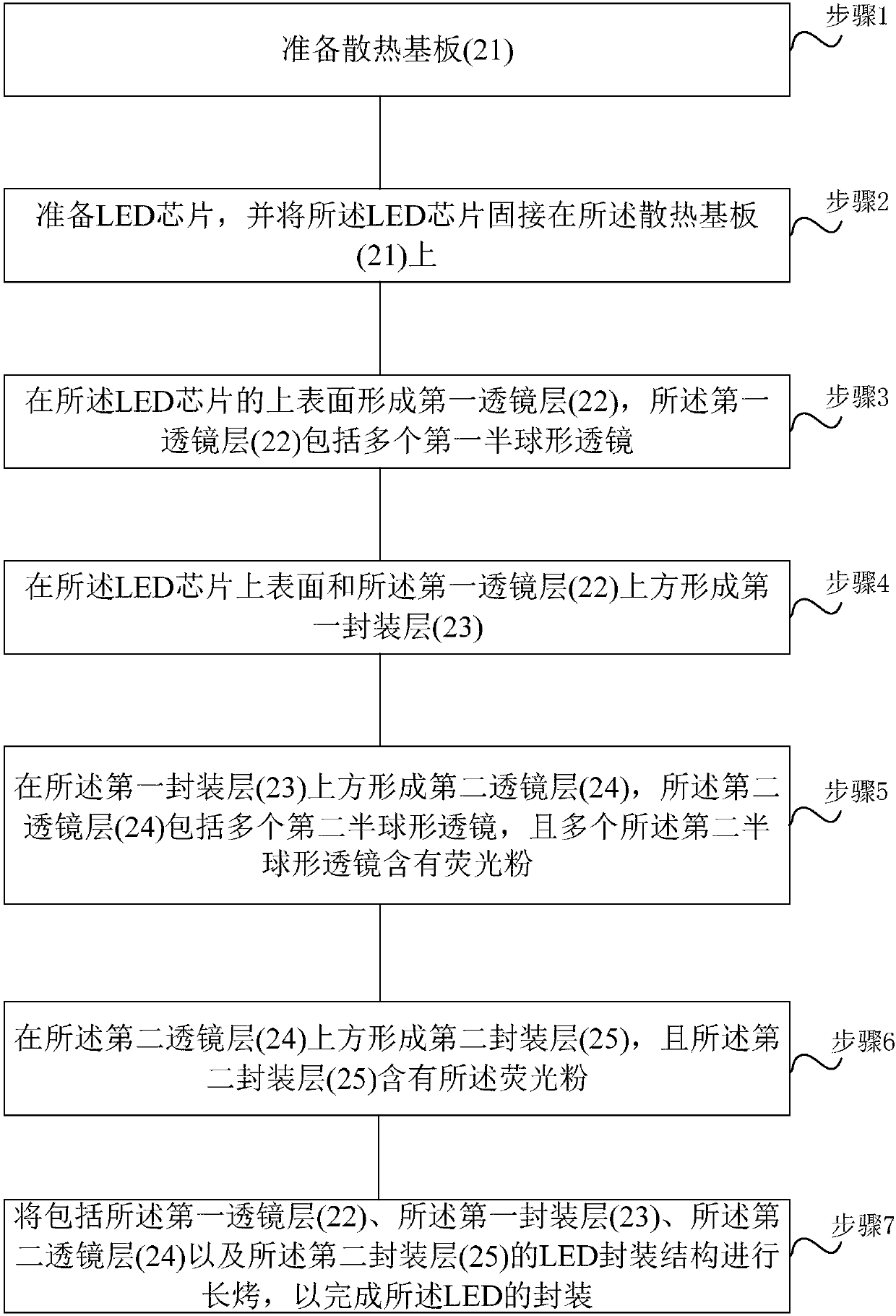
[0053] Embodiments of the present invention provide an LED packaging method, which includes:
[0054] Step 1. Prepare the heat dissipation substrate 21;
[0055] Step 2, prepare LED chips, and fix the LED chips on the heat dissipation substrate 21;
[0056] Step 3, forming a first lens layer 22 on the upper surface of the LED chip, and the first lens layer 22 includes a plurality of first hemispherical lenses;
[0057] Step 4, forming a first encapsulation layer 23 on the upper surface of the LED chip and above the first lens layer 22;
[0058]Step 5, forming a second lens layer 24 above the first encapsulation layer 23, the second lens layer 24 includes a plurality of second hemispherical lenses, and the plurality of the second hemispherical lenses contain phosphors;
[0059] Step 6, forming a second encapsulation layer 25 above the second lens layer 24, and the second encapsulation layer 25 contains the phosphor;
[0060] Step 7. Long bake the LED package structure includ...
Embodiment 2
[0091] Please refer to figure 1 , figure 1 This is a flowchart of the LED packaging method provided by the embodiment of the present invention; wherein, on the basis of the above embodiment, the LED packaging method provided by the embodiment of the present invention is described in detail, and the specific steps are as follows:
[0092] Step 1. Prepare the heat dissipation substrate 21;
[0093] Step 11. Select the heat dissipation substrate 21;
[0094] Specifically, a heat dissipation substrate 21 with a thickness of 0.5-10 mm and a solid copper plate is selected, and the heat dissipation substrate 21 is cut into the required size;
[0095] Step 12, cleaning the heat dissipation substrate 21;
[0096] Specifically, clean the stains, especially oil stains, on the heat dissipation substrate 21;
[0097] Step 13, drying the heat dissipation substrate 21;
[0098] Specifically, baking and cleaning the heat-dissipating substrate 21 to keep the heat-dissipating substrate 21 ...
PUM
 Abstract
Description
Claims
Application Information


