Preparation method of multi-layer flexible printed circuit

A flexible circuit board and flexible circuit technology, which is applied in the direction of multi-layer circuit manufacturing, flexible printed circuit board, printed circuit manufacturing, etc. and other problems, to achieve the effect of easy large-scale implementation, low production equipment requirements, and environmental friendliness

Inactive Publication Date: 2018-03-27
SUZHOU NANOGRID TECH
View PDF3 Cites 10 Cited by
  • Summary
  • Abstract
  • Description
  • Claims
  • Application Information

AI Technical Summary

Problems solved by technology

[0004] When a traditional flexible circuit board is prepared as a multi-layer board, it generally starts with the inner layer pattern, and after etching, bonding and pressing, the through hole is usually realized by mechanical drilling or laser drilling, but the buried and blind holes of the circuit It is difficult to achieve through drilling, which limits the development of flexible circuit boards in the direction of high density, high precision and number of layers; in addition, the temperature of the pressing process is relatively high, making flexible circuit boards basically use polyimide high temperature resistant materials, which The mate...

Method used


Image

  • Preparation method of multi-layer flexible printed circuit
  • Preparation method of multi-layer flexible printed circuit
  • Preparation method of multi-layer flexible printed circuit

Examples


preparation example Construction

[0075] Another aspect of the embodiment of the present application provides a method for preparing a multi-layer flexible circuit board comprising:

[0076] 1) providing a flexible substrate, the flexible substrate comprising a first surface and a second surface opposite to the first surface;

[0077] 2) setting a circuit layer as the first circuit layer on the first surface of the flexible substrate;

[0078] 3) setting an insulating medium layer as the first insulating medium layer on the circuit layer;

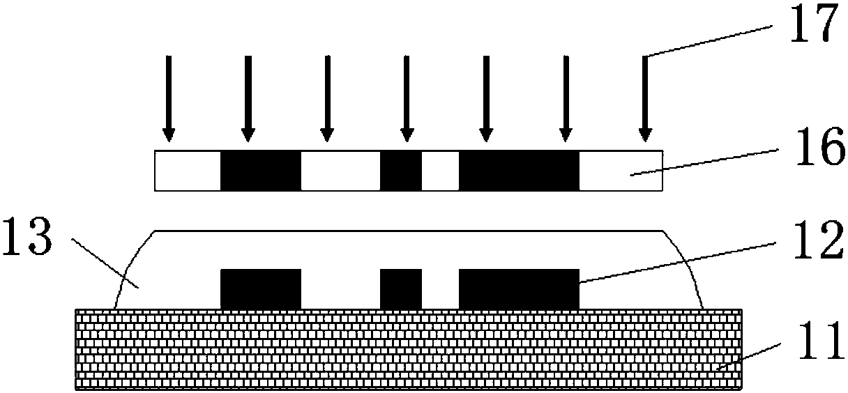
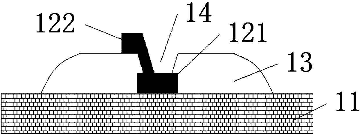
[0079] 4) Processing and forming at least one through hole on the insulating dielectric layer, the openings at both ends of the through hole are respectively arranged on the side surface of the insulating dielectric layer opposite to the first surface and the insulating dielectric layer and the first surface. the surface on the opposite side of the surface;

[0080] 5) Coating conductive paste or conductive ink on the insulating medium layer, and allowing a part of the co...

Embodiment 1

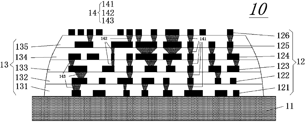
[0161] The multilayer flexible circuit board of this embodiment includes a flexible PET film as a base and a flexible circuit layer arranged on the PET film, and the flexible circuit layer includes a first circuit layer formed on the surface of the PET film, a first Insulating medium layer, second circuit layer, second insulating medium layer, third circuit layer, third insulating medium layer and fourth circuit layer (ie top circuit layer). The flexible circuit layer is also provided with conductive holes prepared by the aforementioned "plug plate" process, and the conductive holes include conductive through-holes that run through the entire flexible circuit layer, and conductive holes that connect the surface circuit layer and the internal circuit layer. Blind holes, conductive buried holes connecting internal circuit layers, etc.

[0162] The preparation process of the multilayer flexible circuit board in this embodiment may include: providing a flexible PET film, adopting ...

Embodiment 2

[0164] The multilayer flexible circuit board of this embodiment includes a flexible PET film as a base and a flexible circuit layer arranged on the PET film, and the flexible circuit layer includes a first circuit layer formed on the surface of the PET film, a first Insulating medium layer, second circuit layer, second insulating medium layer, third circuit layer, third insulating medium layer and fourth circuit layer, fourth insulating medium layer, fifth circuit layer, Five insulating dielectric layers, the sixth circuit layer (that is, the top circuit layer). The flexible circuit layer is also provided with conductive holes prepared by the aforementioned "plug plate" process, and the conductive holes include conductive through-holes that run through the entire flexible circuit layer, and conductive holes that connect the surface circuit layer and the internal circuit layer. Blind holes, conductive buried holes connecting internal circuit layers, etc.

[0165] The preparati...


PUM

PropertyMeasurementUnit
Surface roughnessaaaaaaaaaa
Thicknessaaaaaaaaaa
Thicknessaaaaaaaaaa

Abstract

The invention discloses a preparation method of a multi-layer flexible printed circuit. The preparation method of the multi-layer flexible printed circuit comprises the following steps: providing flexible base materials of a first surface and a second surface which are arranged back to back; setting a first circuit layer on the first surface; setting a first insulating medium layer on the first circuit layer; processing and forming a number of through-holes on the first insulating medium layer; coating a conductive slurry or ink on the insulating medium layer, and making a part of the conductive slurry or ink flow into the through-holes and contact with the first circuit layer; then solidifying the conductive slurry or ink to form a second conductive layer on the insulating medium layer and form a conductive filler which can at least connect the first and second circuit layers electrically in the through-holes; and repeating the above operations until more than two insulating layers and more than three circuit layers are formed. The preparation method of the multi-layer flexible printed circuit is simple and easy to implement, has the advantages of good controllability, low cost and friendly environment, and benefits large-scale implementation; and the obtained printed circuit has super thin and soft characteristics.

Description

technical field [0001] The application specifically relates to a preparation process of a multilayer flexible circuit board, which belongs to the technical field of circuit board manufacturing. Background technique [0002] With the advancement of electronic technology, electronic products are developing toward diversification, intelligence, and flexibility. The most typical representative is the rise of smart wearable electronic products, which put forward higher requirements for the circuit boards. Flexible circuit board, also known as flexible circuit board, flexible circuit board, referred to as soft board or FPC (Flexible Printed Circuit), has the characteristics of high wiring density, light weight, thin thickness, and bendability, and is especially suitable for complex shapes. , Electronic products with narrow internal space or complex human morphology. [0003] Flexible circuit boards are divided into single-sided, double-sided and multi-layer boards, and the base m...

Claims


Application Information

Patent Timeline
IPC IPC(8): H05K3/46H05K3/42H05K1/11
CPCH05K3/465H05K1/115H05K1/118H05K3/429H05K2201/05H05K2201/095
Inventor 张克栋顾唯兵李亚邦崔铮
Owner SUZHOU NANOGRID TECH
Why Eureka
Try Eureka