Pulse width modulation (PWM) control-based switch power supply driving circuit

A technology of drive circuit and timing control circuit, which is applied in the direction of high-efficiency power electronic conversion, electrical components, output power conversion devices, etc., can solve problems such as large reverse recovery loss, and achieve the effect of reducing reverse recovery loss

Active Publication Date: 2018-03-30
LEN TECH LTD
View PDF8 Cites 3 Cited by
  • Summary
  • Abstract
  • Description
  • Claims
  • Application Information

AI Technical Summary

Problems solved by technology

Similarly, when the inductor current flowing out of the VSW node is negative, the body diode of the upper transistor LS_FET will conduct and bring relatively large reverse recovery loss

Method used


Image

  • Pulse width modulation (PWM) control-based switch power supply driving circuit
  • Pulse width modulation (PWM) control-based switch power supply driving circuit
  • Pulse width modulation (PWM) control-based switch power supply driving circuit

Examples


Embodiment 2

[0084] combine Figure 10 , to describe Embodiment 2 of the present invention in detail, but does not limit the claims of the present invention in any way.

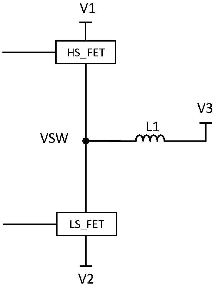
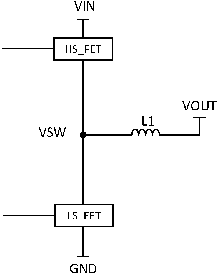
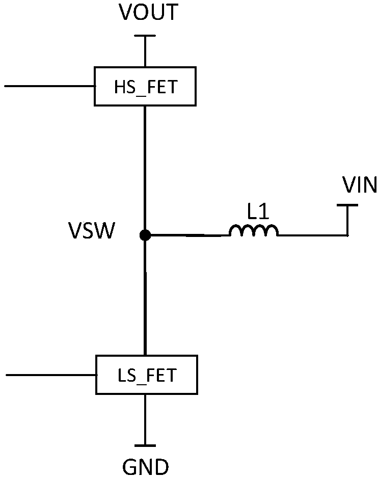
[0085] in such as Figure 6 In the basic construction unit of the switching power supply circuit shown, when the inductor current flowing out of the VSW node is negative, the body diode of the HS_FET will conduct and bring a relatively large The reverse recovery loss, so HS_FET needs a new drive circuit to reduce the reverse recovery loss caused by the HS_FET body diode.

[0086] Such as Figure 10 As shown, a switching power supply drive circuit based on PWM control. The switching power supply circuit at least includes an upper MOS transistor HS_FET, a lower MOS transistor HS_FET and an inductor L1. The gate of HS_FET is used to access the driving signal of HS_FET, and the gate of LS_FET is used for When the LS_FET drive signal is connected, the source of HS_FET, the drain of LS_FET are connected to one end of L1, the...


PUM


Abstract

The invention belongs to the technical field of switch power supply control, and particularly relates to a switch power supply driving circuit for reducing loss of metal-oxide-semiconductor (MOS) tubediode in a switch power supply circuit. The switch power supply circuit at least comprises an upper MOS tube, a lower MOS tube and an inductor, a driving circuit comprises an upper MOS tube driving power supply, a lower MOS tube driving power supply, a time sequence control circuit, an upper MOS tube driving circuit and a lower MOS tube driving circuit, the upper MOS tube driving circuit and/or the lower MOS tube driving circuit comprises four transistors and a switch, the conduction of a lower MOS tube diode is effectively prevented during the conversion process from switch-off of the lowerMOS tube to the conduction of the upper MOS tube and/or the conduction of an upper MOS tube diode is effectively prevented during the conversion process from switch-off of the upper MOS tube diode tothe conduction of the lower MOS tube, or only a small part of current flows through a body diode, so that reverse recovery loss caused by the body diode is effectively reduced.

Description

technical field [0001] The technical field of switching power supply control of the present invention, in particular, relates to a switching power supply drive circuit for reducing loss of MOS transistor body diodes in a switching power supply circuit based on PWM control. Background technique [0002] Such as figure 1 As shown, it is the basic construction unit of the existing PWM-controlled switching power supply, V1>V2 is defined, the MOSFET connected to V1 is called HS_FET, and the MOSFET connected to V2 is called LS_FET. When the input (VIN), output (VOUT) and ground (GND) of the system are respectively assigned to V1, V2, and V3, different types of switching power supplies can be formed, such as figure 2 and image 3 As shown, they are buck converter and boost converter respectively, such as Figure 4 and Figure 5 Two types of inverting buck-boost converters are shown. [0003] Such as Figure 6 As shown, it is the basic construction unit of a switching power s...

Claims


Application Information

Patent Timeline
Patent Type & Authority Applications(China)
IPC IPC(8): H02M1/08
CPCH02M1/08H02M1/0051Y02B70/10
Inventor 陈劲泉陆玮倪川
Owner LEN TECH LTD
Why Eureka
Try Eureka