Array substrate, manufacturing method of array substrate, display panel and display device

A technology for array substrates and display areas, applied to display panels and display devices, its manufacturing method, and the field of array substrates, which can solve the problems of large signal transmission delays and affecting display effects, etc.

Active Publication Date: 2018-04-06
SHANGHAI AVIC OPTOELECTRONICS
View PDF9 Cites 16 Cited by
  • Summary
  • Abstract
  • Description
  • Claims
  • Application Information

AI Technical Summary

Problems solved by technology

[0005] Embodiments of the present invention provide an array substrate, a manufacturing method thereof, a display panel, and a display device, w

Method used


Image

  • Array substrate, manufacturing method of array substrate, display panel and display device
  • Array substrate, manufacturing method of array substrate, display panel and display device
  • Array substrate, manufacturing method of array substrate, display panel and display device

Examples


Embodiment Construction

[0040] To solve the problem in the prior art that the signal transmission delay of the multiplexer is large and affects the display effect, the embodiments of the present invention provide an array substrate, a manufacturing method thereof, a display panel and a display device.

[0041] The specific implementation manners of the array substrate, the manufacturing method thereof, the display panel and the display device provided by the embodiments of the present invention will be described in detail below with reference to the accompanying drawings. The thickness and shape of each film layer in the drawings do not reflect the real scale, and the purpose is only to illustrate the content of the present invention.

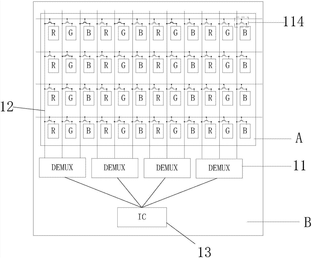
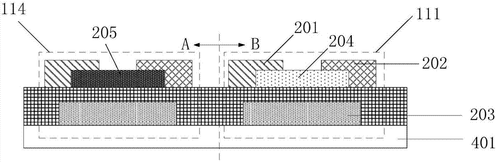
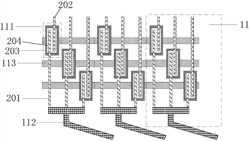
[0042] In a first aspect, an embodiment of the present invention provides an array substrate, Figure 1a is a top view of the array substrate, figure 2 is a partially enlarged view of the multiplexer in the array substrate, such as Figure 1a and figure 2 As shown,...


PUM


Abstract

The invention discloses an array substrate, a manufacturing method of the array substrate, a display panel and a display device. The array substrate comprises multiple first thin film transistors which are arranged in a display area, wherein each first thin film transistor comprises a first active layer and the material of the first active layer includes amorphous silicon; and at least one multiplexer which is arranged in a non-display area. The multiplexer comprises multiple second thin film transistor, one input end and multiples control signal lines. The first electrode of each second thinfilm transistor is electrically connected with the input end, the second electrode of each second thin film transistor is electrically connected with different data lines in the display area, and thecontrol end of each second thin film transistor is electrically connected with different control signal lines. Each second thin film transistor comprises a second active layer, and the material of thesecond active layer includes polysilicon. The material of the second active layer includes polysilicon so that the number of leads connected with the data lines can be reduced on the basis of meetingthe signal transmission speed of the data lines and the frame can be reduced.

Description

technical field [0001] The invention relates to the field of display technology, in particular to an array substrate, a manufacturing method thereof, a display panel and a display device. Background technique [0002] With the continuous development of display technology, display screens or touch screens have been widely used in people's lives. Among them, Liquid Crystal Display (LCD) has the characteristics of small size, low power consumption, and no radiation, and occupies an important position in the market. status. Organic Light-Emitting Diode (OLED) has the advantages of self-luminescence, fast response, wide viewing angle, high brightness, bright color, light and thin, etc., and has been widely used in the market. [0003] Thin Film Transistor (TFT) is an important component in various circuits of display devices, and has been widely used in Liquid Crystal Display (LCD) and Organic Light-Emitting Diode (OLED). In the prior art, since the manufacturing process of amo...

Claims


Application Information

Patent Timeline
IPC IPC(8): H01L27/32H01L27/12
CPCH01L27/1251H10K59/35H10K59/1213
Inventor 金慧俊
Owner SHANGHAI AVIC OPTOELECTRONICS
Why Eureka
Try Eureka