Light emitting diode epitaxial wafer preparation method and light emitting diode epitaxial wafer

A technology for light-emitting diodes and epitaxial wafers, applied in electrical components, circuits, semiconductor devices, etc., can solve the problems of poor consistency of light-emitting diode epitaxial wafers, and achieve the effects of avoiding different photoelectric properties, improving consistency, and reducing time consumption.

Active Publication Date: 2018-04-06
HC SEMITEK ZHEJIANG CO LTD
View PDF3 Cites 4 Cited by
  • Summary
  • Abstract
  • Description
  • Claims
  • Application Information

AI Technical Summary

Problems solved by technology

[0006] In order to solve the problem of poor consistency of light-emitting diode epitaxial wafers in the prior art, an embodiment of the present invention provides a method for preparing a light-emitting diode epitaxial wafer and a light-emitting diode epitaxial wafer.

Method used


Image

  • Light emitting diode epitaxial wafer preparation method and light emitting diode epitaxial wafer
  • Light emitting diode epitaxial wafer preparation method and light emitting diode epitaxial wafer
  • Light emitting diode epitaxial wafer preparation method and light emitting diode epitaxial wafer

Examples


Embodiment 1

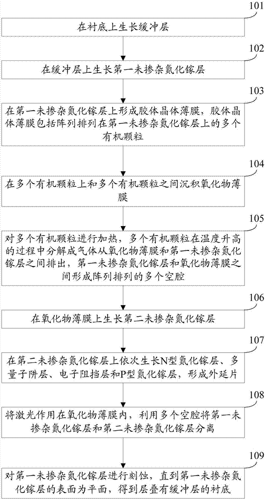
[0040] The embodiment of the present invention provides a method for preparing a light-emitting diode epitaxial wafer, see figure 1 , the preparation method comprises:

[0041] Step 101: growing a buffer layer on a substrate.

[0042] Specifically, the substrate can be sapphire with [0001] crystal orientation.

[0043] Optionally, before step 101, the preparation method may also include:

[0044] The temperature is controlled at 1000° C. to 1200° C., the substrate is annealed in a hydrogen atmosphere for 8 minutes, and nitriding treatment is performed to clean the substrate.

[0045] Specifically, this step 101 may include:

[0046] The temperature is controlled at 400° C. to 600° C., the pressure is 400 Torr to 600 Torr, and a gallium nitride layer with a thickness of 15 nm to 35 nm is grown on the substrate to form a buffer layer.

[0047] Optionally, after step 101, the preparation method may further include:

[0048] The temperature is controlled to be 1000° C. to 120...

Embodiment 2

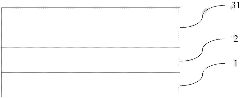
[0097] The embodiment of the present invention provides a method for preparing a light-emitting diode epitaxial wafer, see image 3 , the preparation method comprises:

[0098] Step 201: providing a substrate laminated with a buffer layer.

[0099] Specifically, in step 201, the substrate obtained in step 108 and step 109 in the first embodiment with a buffer layer laminated thereon can be used.

[0100] Step 202: growing a first undoped GaN layer on the buffer layer.

[0101] Specifically, if there is no first undoped gallium nitride layer on the buffer layer stacked on the substrate in step 201, then this step 202 can be the same as step 102 in Embodiment 1, and will not be described in detail here. If the first undoped gallium nitride layer is also laminated on the buffer layer stacked on the substrate in step 201, the thickness of the grown first undoped gallium nitride layer can be correspondingly reduced, so that the grown in step 202 The sum of the thickness of the f...

Embodiment 3

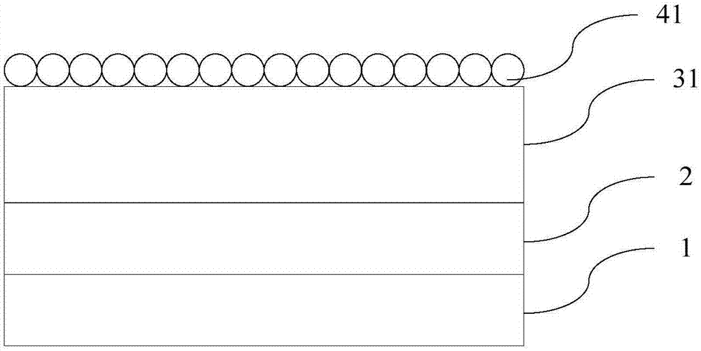
[0119] The embodiment of the present invention provides a light-emitting diode epitaxial wafer, which can be prepared by the preparation method provided in the above-mentioned embodiment 1 or embodiment 2. Specifically, see Figure 4 , the light-emitting diode epitaxial wafer includes a buffer layer, a first undoped gallium nitride layer, a colloidal crystal film, an oxide film, a second undoped gallium nitride layer, an N-type nitride layer, and a buffer layer sequentially stacked on the substrate. Gallium nitride layer, multi-quantum well layer, electron blocking layer and P-type gallium nitride layer.

[0120] In this embodiment, the colloidal crystal thin film includes a plurality of organic particles arrayed on the first undoped gallium nitride layer, and the oxide thin film is disposed on and between the plurality of organic particles.

[0121] Optionally, the diameter of the organic particles may be 0.5 μm˜1.8 μm. If the diameter of the organic particles is less than ...


PUM

PropertyMeasurementUnit
Diameteraaaaaaaaaa
Thicknessaaaaaaaaaa
Thicknessaaaaaaaaaa

Abstract

The invention discloses a light emitting diode epitaxial wafer preparation method and a light emitting diode epitaxial wafer, which belong to the technical field of semiconductors. The method comprises steps: a first un-doped gallium nitride layer grows on a buffer layer which is stacked on a substrate; a colloidal crystal thin film is formed on the first un-doped gallium nitride layer, wherein the colloidal crystal thin film comprises multiple organic particles arranged in an array; an oxide thin film is deposited on the multiple organic particles and between the multiple organic particles; the multiple organic particles are heated, the multiple organic particles are decomposed to a gas during a temperature rise process and the gas is exhausted from between the oxide thin film and the first un-doped gallium nitride layer, and multiple cavities which are arranged in an array are formed between the first un-doped gallium nitride layer and the oxide thin film; a second un-doped gallium nitride layer grows on the oxide thin film; and an N-type gallium nitride layer, multiple quantum well layers, an electron barrier layer and a P-type gallium nitride layer grow on the second un-doped gallium nitride layer sequentially, and an epitaxial wafer is formed. Thus, the epitaxial wafer consistency is improved.

Description

technical field [0001] The invention relates to the technical field of semiconductors, in particular to a method for preparing a light-emitting diode epitaxial wafer and the light-emitting diode epitaxial wafer. Background technique [0002] Light Emitting Diode (English: Light Emitting Diode, referred to as: LED) is a semiconductor light emitting device made by using the principle of semiconductor PN junction electroluminescence. The epitaxial wafer is the primary product in the process of manufacturing light-emitting diodes. [0003] The existing epitaxial wafer includes a sapphire substrate and a buffer layer, an undoped gallium nitride layer, an n-type gallium nitride layer, a multi-quantum well layer, an electron blocking layer and a p-type gallium nitride layer stacked on the sapphire substrate in sequence. Floor. The electrons provided by the N-type gallium nitride layer and the holes provided by the P-type gallium nitride layer can be injected into the multi-quantu...

Claims


Application Information

Patent Timeline
IPC IPC(8): H01L33/00H01L33/12
CPCH01L33/0093H01L33/12
Inventor 郭炳磊王群葛永晖吕蒙普胡加辉李鹏
Owner HC SEMITEK ZHEJIANG CO LTD
Why Eureka
Try Eureka