Biaser and manufacturing method thereof

A manufacturing method and biaser technology, applied in semiconductor/solid-state device manufacturing, inductors, capacitors, etc., can solve problems such as inability to completely eliminate the influence of series resonance, uneven broadband, etc., and achieve freedom of choice, large inductance density, Effect of Reducing Parasitic Capacitance

Active Publication Date: 2020-05-01
NAT CENT FOR ADVANCED PACKAGING
View PDF4 Cites 0 Cited by
  • Summary
  • Abstract
  • Description
  • Claims
  • Application Information

AI Technical Summary

Problems solved by technology

[0004] Therefore, the technical problem to be solved by the present invention is to overcome the defect that the broadband is not flat in the prior art, and the influence of series resonance on the device cannot be completely eliminated by adjusting the inductance and capacitance parameters, thereby providing a bias device and a manufacturing method

Method used


Image

  • Biaser and manufacturing method thereof
  • Biaser and manufacturing method thereof
  • Biaser and manufacturing method thereof

Examples


Embodiment 1

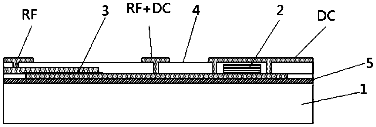
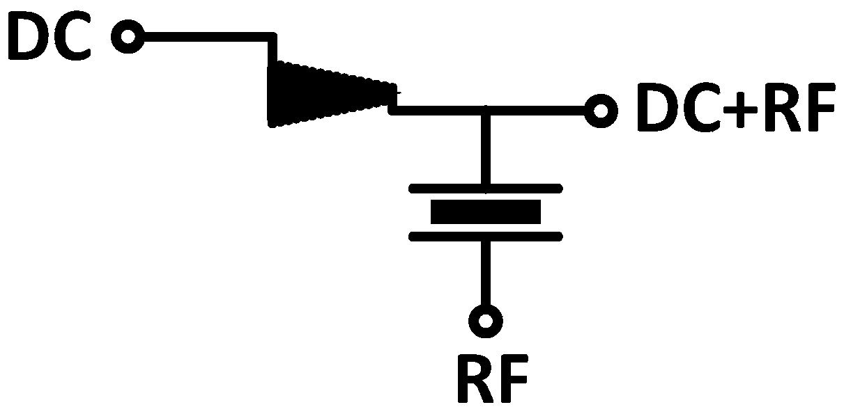
[0050] The embodiment of the present invention provides a bias device, which can be applied to various circuits and systems requiring AC and DC isolation. like figure 1 As shown, the bias device mainly includes: a wafer substrate 1 , an inductor part 2 , a capacitor part 3 and a first insulating layer 4 .

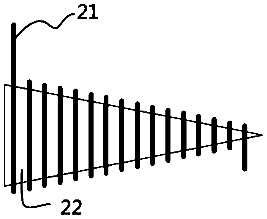
[0051] Wherein, the above-mentioned inductor part 2 and capacitor part 3 are arranged on the wafer substrate 1 . In a preferred embodiment, the inductor part 2 is a tapered inductor, such as figure 2 As shown, the inductance part 2 includes: a wound coil 21 and a conical thin-film magnetic core 22, the wound coil 21 is evenly wound on the conical thin-film magnetic core 22; the wound coil 21 is generally made of high conductivity material, such as copper. The tapered thin-film magnetic core 22 is generally made of high-frequency ferrite or high-performance magnetic thin-film materials such as CoZrTa, CoZrTaB, and CoZrO.

[0052] The first insulating layer 4 covers the waf...

Embodiment 2

[0057] An embodiment of the present invention provides a method for manufacturing a bias device, such as Figure 4 shown, including the following steps:

[0058] Step S1: if Figure 5 As shown, a second insulating layer 5 is formed on the surface of the wafer substrate 1 .

[0059] Step S2 : forming an inductance part 2 and a capacitor part 3 on the wafer substrate 1 with a predetermined distance apart, and the inductance part 2 is a tapered inductor.

[0060] In a preferred embodiment, the above-mentioned step S2, the step of forming the inductance part 2 and the capacitance part 3, such as Image 6 shown, including:

[0061] Step S21 : forming the inductor lower layer coil 211 and the capacitor lower electrode plate 31 on the second insulating layer. In the embodiment of the present invention, such as Figure 7 As shown, the inductance lower coil 211 and the capacitor lower electrode plate 31 are formed in the middle part of the second insulating layer 5, and the two si...


PUM


Abstract

The present invention discloses a bias tee and a manufacturing method thereof. The bias tee comprises a wafer substrate, an induction portion, a capacitance portion and a first insulation layer. The induction portion and the capacitance portion are arranged on the wafer substrate, and the induction portion is a taper inductor; the induction portion and the capacitance portion are coated with the first insulation layer; the first insulation layer is provided with an electrode interface, and the electrode interface comprises a radio frequency interface, a direct current bias interface and a radio frequency and direct current interface; the direct current bias interface is connected with a first end of the induction portion, the radio frequency and direct current interface is connected with asecond end of the induction portion, a first end of the capacitance portion is connected between the radio frequency and direct current interface and the first end of the induction portion, and a second end of the capacitance portion is connected with the radio frequency interface. The bias tee and the manufacturing method thereof can achieve rapid large-scale production of a chip bias tee and can perform chip integration with other related devices, employ the taper inductor to achieve reduction of parasitic capacitance and can achieve preparation of a flat broadband bias tee.

Description

technical field [0001] The invention relates to the field of semiconductor packaging, in particular to a bias device and a manufacturing method. Background technique [0002] For any microwave devices and systems that require DC power supply, appropriate measures are required to prevent interference between microwave energy and DC power supply. Generally, a Bias-Tee biaser is used to eliminate the mutual interference between the DC source and the RF source. The biaser generally uses the method of inductance and capacitance to isolate AC and DC. The AC signal cannot pass through the inductor, and the DC signal cannot pass through the capacitor. In the traditional bias device, if only a single inductor is used, the bias device can only obtain a narrow operating frequency band. In order to achieve broadband, multi-stage inductors are used in series, and the DC terminal uses an inductor with a large inductance value. The AC terminal adopts an inductance with a small inductance ...

Claims


Application Information

Patent Timeline
Patent Type & Authority Patents(China)
IPC IPC(8): H01L27/13H01L21/84H01L49/02
CPCH01L21/84H01L27/13H01L28/10H01L28/40
Inventor 周予虹孙鹏司马格
Owner NAT CENT FOR ADVANCED PACKAGING
Why Eureka
Try Eureka