Manufacturing process of high-fall stepped circuit board

A production process and circuit board technology, which is applied in the field of production process of high-drop ladder circuit boards, can solve the problems of affected positioning accuracy, reduced production efficiency, unsuitable for mass production, etc., so as to save process labor costs and facilitate mass production. The effect of making it easy to press and typesetting

Inactive Publication Date: 2018-04-20
JIANGMEN SUNTAK CIRCUIT TECH +1
View PDF6 Cites 14 Cited by
  • Summary
  • Abstract
  • Description
  • Claims
  • Application Information

AI Technical Summary

Problems solved by technology

[0003] The manufacturing methods of the above-mentioned stepped slabs have the following defects: (1) The tolerance of the thickness H of the finished plate is generally + / -10%. Plate thickness tolerance, machine accuracy tolerance, etc. are superimposed (generally + / -0.1MM, limit capacity + / -0.075MM can be achieved), and it is difficult to guarantee the tolerance of + / -0.05MM for the excess thickness T; (2) The excess at the stepped groove The thick platform is uneven, glass fiber is exposed, etc.; (3) The larger the drop of the stepped groove, the more difficult it is to achieve the excess thickness tolerance of + / -0.05MM controlled by deep milling; (4) The uneven pressing pressure on the stepped platform is easy Cause connection breakage; (5) Teflon gasket embedded is easy to misplace, especially for small-sized gaskets, the positioning accuracy is affected, and tweezers need to be used to assist placement, etc.; (5) Teflon gasket embedded due to needs Manual placement is time-consuming and labor-intensive, which reduces production efficiency and is not suitable for mass production; (6) Teflon gaskets are embedded due to the elasticity of the gasket itself, and there is a risk of drilling deviation on it; ( 7) When using the NOflow PP (non-flowing PP sheet) window opening method, it is easy to produce depressions at the step position, which makes it difficult to ensure the flatness of the platform, which affects the actual residual thickness of the platform

Method used


Image

  • Manufacturing process of high-fall stepped circuit board
  • Manufacturing process of high-fall stepped circuit board
  • Manufacturing process of high-fall stepped circuit board

Examples


Embodiment

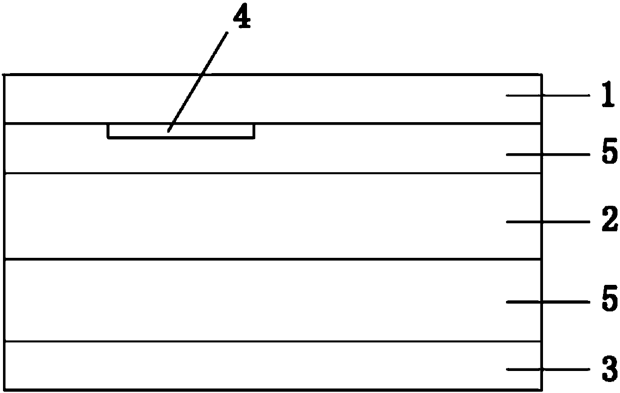
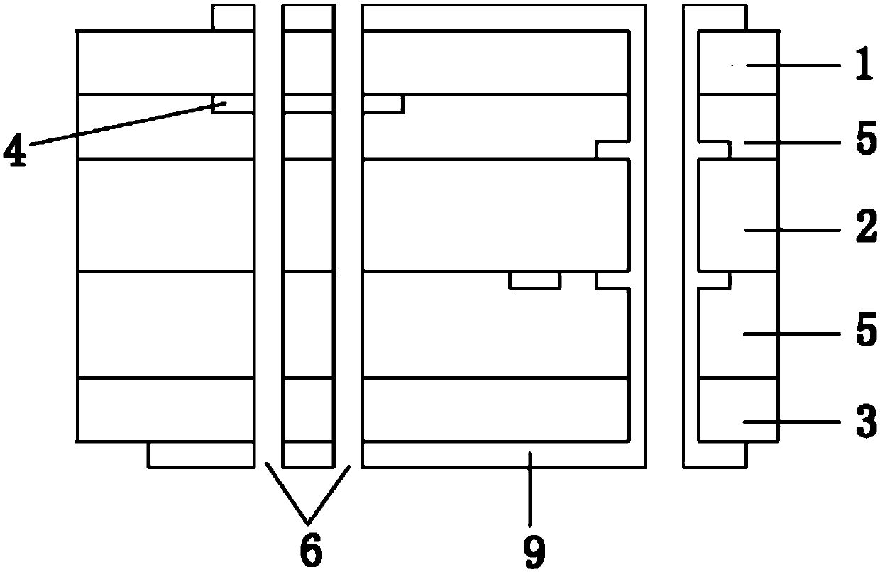
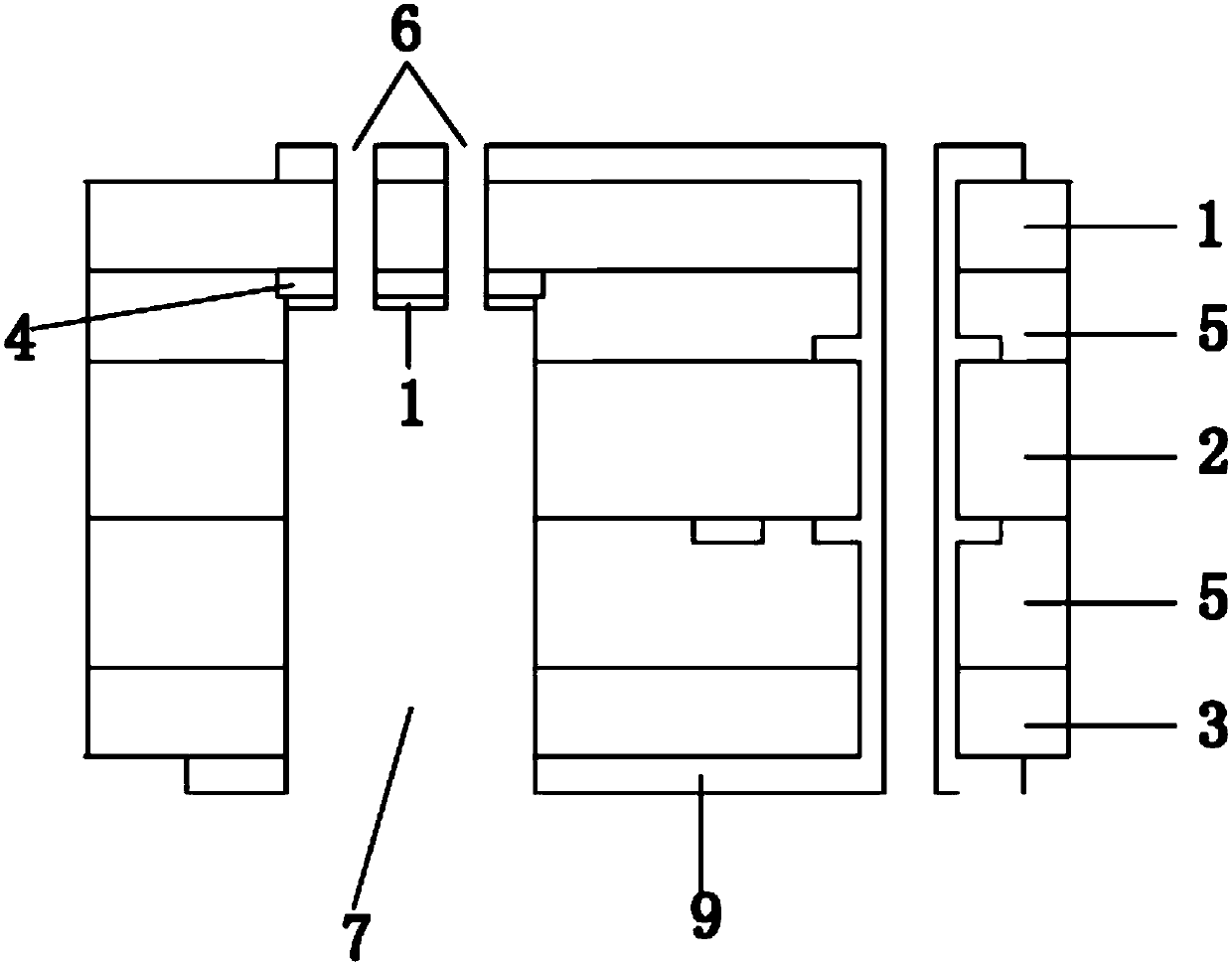
[0025] Such as Figure 1 to Figure 4 As shown, the manufacturing process of a high-drop ladder circuit board shown in this embodiment includes core board one, core board two and core board three, and the manufacturing method includes the following processing steps in sequence:

[0026] (1) Cutting: According to the board size 320mm×420mm, core board 1, core board 2, core board 3 3 are cut out, and the thickness of core board 1 and core board 3 are both 0.15mm. The thickness of the outer layer copper surface of core board 1 and core board 3 3 is 0.5OZ, the thickness of core board 2 2 is 0.71mm, and the thickness of the outer layer copper surface of core board 2 2 is 1OZ.

[0027] (2), inner layer drilling: drill pattern positioning holes and riveting positioning holes at the corresponding positions of core plate one 1, core plate two 2 and core plate three 3 respectively.

[0028] (3), making the inner layer circuit (negative film process): according to the pattern positioning...


PUM


Abstract

The invention discloses a manufacturing process of a high-fall stepped circuit board. The manufacturing process comprises the steppeds of: manufacturing inner-layer circuits on a plurality of core boards separately, and manufacturing an auxiliary copper skin at a position corresponding to a stepped platform when the inner-layer circuit is manufactured on one of the core board; laminating the plurality of core boards into a multi-layer board; performing intermediate processing on the multi-layer board sequentially; performing depth-control groove milling inwardly at a position corresponding tothe stepped platform on the multi-layer board to a position 0.1 mm +/- 0.075 mm away from the auxiliary copper skin beform outer layer etching during the manufacturing process of an outer layer circuit, and forming the stepped platform after removing a cover; performing ablation on a residual dielectric layer at the bottom part at the stepped platform by means of laser; manufacturing the outer layer circuit through etching and removing the auxiliary copper skin at the stepped platform at the same time; and performing post-procedure processing on the multi-layer board to manufacture the high-fall stepped circuit board. According to the manufacturing process, the core board thickness is adopted to make a residual thickness step, the residual thickness tolerance of the stepped platform aftermolding and milling is ensured to meet requirements, the high-precision residual thickness tolerance is ensured to be realized, and the production efficiency can be improved.

Description

technical field [0001] The invention relates to the technical field of printed circuit board production, in particular to a production process of a stepped circuit board with a high drop. Background technique [0002] A stepped board refers to a multilayer printed circuit board with stepped grooves. At present, the production process of stepped circuit boards is mainly: forming inner layer boards through material cutting, inner layer pattern transfer and etching; pressing each inner layer board to form multilayer boards; Board electroplating, outer layer graphics, graphic electroplating, outer layer etching and coating solder resist layer to form a multi-layer circuit board with outer layer circuits; finally surface treatment and forming, and after forming, control the depth of milling slots to form a ladder After the final inspection, the finished product is made; the second method is to open the window on the inner plate first, and then open the outer cover to form a step...

Claims


Application Information

Patent Timeline
Patent Type & Authority Applications(China)
IPC IPC(8): H05K3/46
Inventor 张国城彭卫红刘东翟青霞黄宏波
Owner JIANGMEN SUNTAK CIRCUIT TECH
Why Eureka
Try Eureka