
Wafer bonding method and bonding device thereof

A wafer bonding and wafer technology, which is applied in the fields of electrical components, semiconductor/solid-state device manufacturing, circuits, etc., can solve the problem of lower bonding yield, large gap in wafer thermal expansion coefficient, and gallium nitride-based semiconductor device yield. Reduce other problems, achieve the effect of improving efficiency and reliability

Active Publication Date: 2018-04-24
ZING SEMICON CORP
View PDF8 Cites 4 Cited by
  • Summary
  • Abstract
  • Description
  • Claims
  • Application Information

AI Technical Summary

Problems solved by technology

However, due to the large gap between the thermal expansion coefficients of the wafers during bonding, there is a large stress between the two wafers after bonding, which reduces the bonding yield and leads to a decrease in the yield of GaN-based semiconductor devices.

Method used


Image

  • Wafer bonding method and bonding device thereof
  • Wafer bonding method and bonding device thereof
  • Wafer bonding method and bonding device thereof

Examples


Embodiment Construction

[0023] In order to make the content of the present invention clearer and easier to understand, the content of the present invention will be further described below in conjunction with the accompanying drawings. Of course, the present invention is not limited to this specific embodiment, and general replacements known to those skilled in the art are also covered within the protection scope of the present invention.

[0024] Secondly, the present invention is described in detail by means of schematic diagrams. When describing the examples of the present invention in detail, for the convenience of illustration, the schematic diagrams are not partially enlarged according to the general scale, which should not be used as a limitation of the present invention.

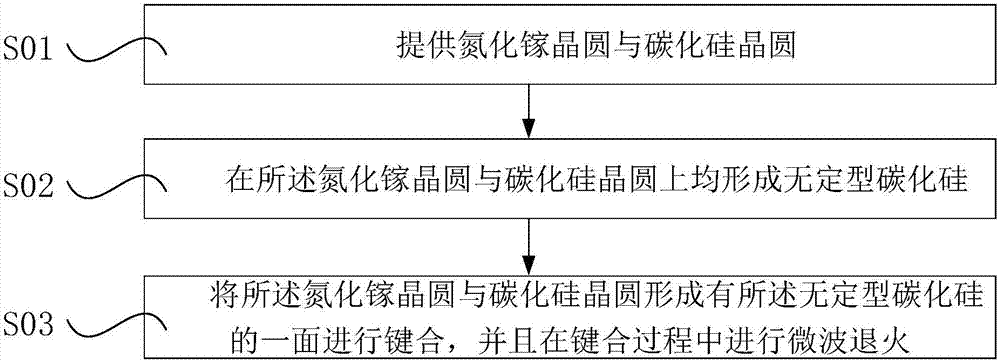
[0025] The core idea of ​​the present invention is: form amorphous silicon carbide on both the gallium nitride wafer and the silicon carbide wafer, and carry out the Bonding, microwave annealing is performed during the bondi...


PUM


Abstract

The invention provides a wafer bonding method and a bonding device thereof. The wafer bonding method comprises the steps of: providing a gallium nitride wafer and a silicon carbide wafer; forming amorphous silicon carbide on the gallium nitride wafer and the silicon carbide wafer; and bonding the surfaces, on which the amorphous silicon carbide is formed, of the gallium nitride wafer and the silicon carbide wafer, and performing microwave annealing during the bonding process. According to the wafer bonding method, the amorphous silicon carbide on the gallium nitride wafer and the silicon carbide wafer is converted into crystalline silicon carbide through microwave annealing, thus the gallium nitride wafer and the silicon carbide wafer are bonded, the bonding efficiency is improved, and thereliability of gallium-nitride-based semiconductor device is improved.

Description

technical field [0001] The invention relates to the field of semiconductor manufacturing, in particular to a wafer bonding method and a bonding device thereof. Background technique [0002] Gallium nitride (GaN)-based semiconductors have excellent material properties, such as large energy gap, high thermal and chemical stability, high electron saturation velocity, and the like. In addition, electronic devices using gallium nitride-based semiconductors have various advantages, such as high breakdown electric field, high maximum current density, stable operating characteristics at high temperature, and the like. Due to such material properties, gallium nitride-based semiconductors can be applied not only to optical devices but also to high-frequency and high-power electronic devices and high-power devices. [0003] Because it is difficult to obtain a good-quality gallium nitride single crystal substrate, sapphire, which has a small lattice mismatch and thermal mismatch with g...

Claims


Application Information

Patent Timeline
Patent Type & Authority Applications(China)
IPC IPC(8): H01L21/18H01L21/268H01L21/67
CPCH01L21/187H01L21/268H01L21/67115H01L21/67121
Inventor 三重野文健
Owner ZING SEMICON CORP
Learn More