

Wavelength Division Mode Division Hybrid Multiplexer Based on Photonic Crystal and Nanowire Waveguide
A photonic crystal and multiplexer technology, applied in optical waveguides, light guides, instruments, etc., can solve the problems of technical difficulty and cost increase, increase system energy consumption, etc., and achieve a large application wavelength range, small channel crosstalk, and device size. small effect
Active Publication Date: 2019-10-01
NANJING UNIV OF POSTS & TELECOMM
View PDF5 Cites 0 Cited by
- Summary
- Abstract
- Description
- Claims
- Application Information
AI Technical Summary
Problems solved by technology
If we want to further increase the capacity of the optical fiber transmission system on the basis of these traditional multiplexing methods, the technical difficulty and cost will be greatly increased, and the energy consumption of the system will also be increased.
Method used
View moreImage
Smart ImageViewing Examples

Examples
Embodiment Construction
Login to View More PUM
 Abstract
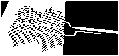
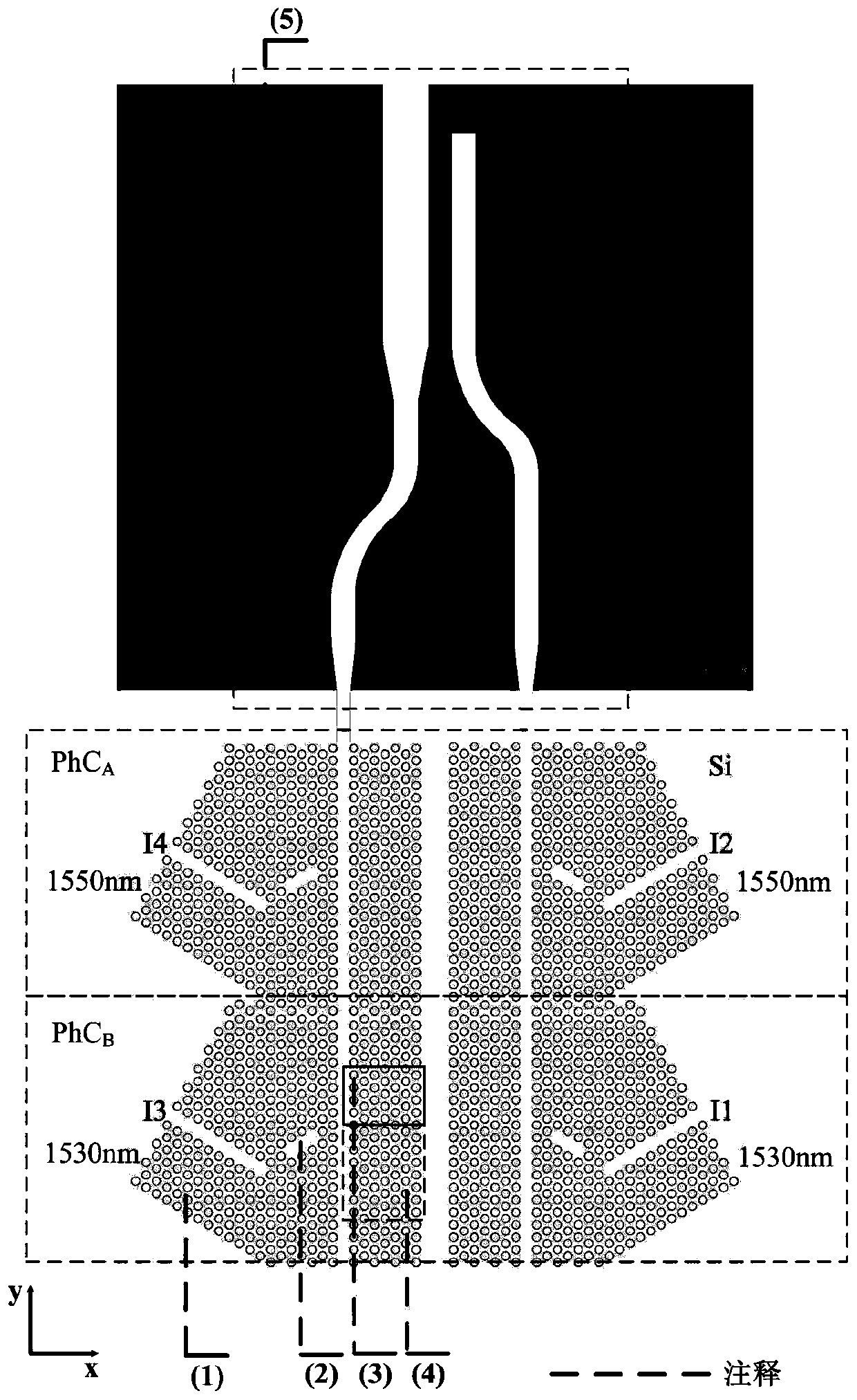
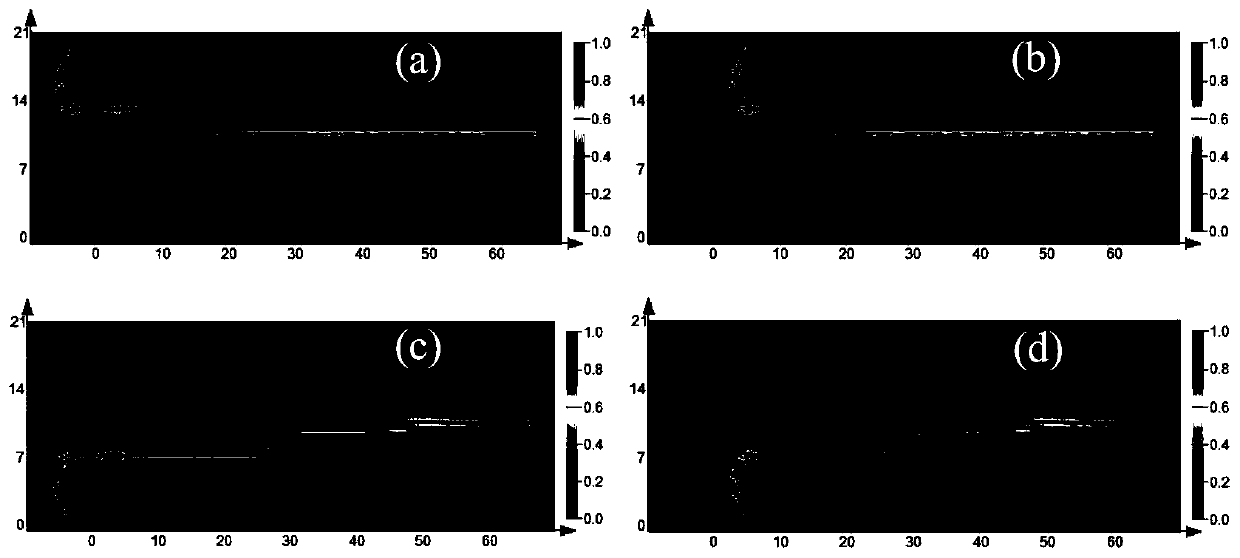
The invention is a wavelength division and mode division hybrid multiplexer based on photonic crystal and nanowire waveguide. A two-dimensional triangular lattice photonic crystal filter (1) is an air-hole photonic crystal plate structure periodically distributed along an X-Y plane, and uses silicon as a host material. An L3-type resonant cavity (2) is formed by removing three air holes. Narrow waveguide structural regions I and II are formed by integrally translating the air holes on a side of the photonic crystal waveguide. A nanowire mode division multiplexer (5) uses silicon as a host material, uses silicon dioxide as a substrate material, and uses asymmetrical directional coupling structure. By using the coupling effect of the microcavity and the waveguide, a download filtering function for a specific-frequency light wave is realized. On this basis, in combination with the nanowire waveguide mode division multiplexing structure, a hybrid multiplexing structure is formed. The wavelength division and mode division hybrid multiplexer can be further cascaded and expanded, can be applied to a C + L band coarse wavelength division (channel spacing of 20 nm) multi-mode (>2) multiplexing system.
Description
technical field The invention relates to a wavelength division mode division hybrid multiplexer based on photonic crystals and nanowire waveguides, in particular to a hybrid multiplexing device for optical communication bands, and relates to the technical fields of optical communication and optical information processing. Background technique With the gradual maturity of technology and industry chain, 100G optical fiber transmission technology has ushered in explosive growth in the global market, and the era of 400G is coming. But just as Moore's Law has failed in the semiconductor industry, the transmission capacity of traditional single-mode optical fiber is gradually approaching the Shannon limit of its channel, and the contradiction between huge bandwidth requirements and limited capacity is increasingly intensified. However, in the current optical fiber transmission network, various multiplexing technologies have already been fully utilized, such as wavelength division ...
Claims
Login to View More Application Information
Patent Timeline
 Patent Type & AuthorityPatents(China)
IPC IPC(8): G02B6/12G02B6/10G02B6/122
Inventor陈鹤鸣庄煜阳胡宇宸季珂
OwnerNANJING UNIV OF POSTS & TELECOMM