Packaging structure for packaging OLED device, and display device

A packaging structure and display device technology, which is applied in the manufacture of electric solid-state devices, semiconductor devices, semiconductor/solid-state devices, etc., can solve the problems of increasing the thickness of OLED devices, easily breaking the inorganic packaging layer, and losing the packaging effect. Effect of thinning, saving barrier layer and reducing thickness

Inactive Publication Date: 2018-05-04
WUHAN CHINA STAR OPTOELECTRONICS SEMICON DISPLAY TECH CO LTD
View PDF10 Cites 3 Cited by
  • Summary
  • Abstract
  • Description
  • Claims
  • Application Information

AI Technical Summary

Problems solved by technology

like figure 2 as shown, figure 1 The range of the stress-strain Axial Strain of the package structure shown is between -2.5 and 2.5, the maximum value reaches 2.5 and the minimum value reaches -2.5, and there is only one position where the stress-strain Axial Strain is 0, that is, the position of the central layer. The inorganic encapsulation layers 11 and 13 in such an encapsulation structure are prone to cracks during the bending process, thereby losing the encapsulation effect.
In addition, the thickness of the barrier layer 14 is generally between tens of microns and hundreds of microns, which also increases the thickness of the entire OLED device.

Method used


Image

  • Packaging structure for packaging OLED device, and display device
  • Packaging structure for packaging OLED device, and display device
  • Packaging structure for packaging OLED device, and display device

Examples


Embodiment Construction

[0022] Hereinafter, embodiments of the present invention will be described in detail with reference to the accompanying drawings. This invention may, however, be embodied in many different forms and should not be construed as limited to the specific embodiments set forth herein. Rather, the embodiments are provided to explain the principles of the invention and its practical application, thereby enabling others skilled in the art to understand the invention for various embodiments and with various modifications as are suited to particular intended uses.

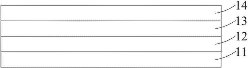
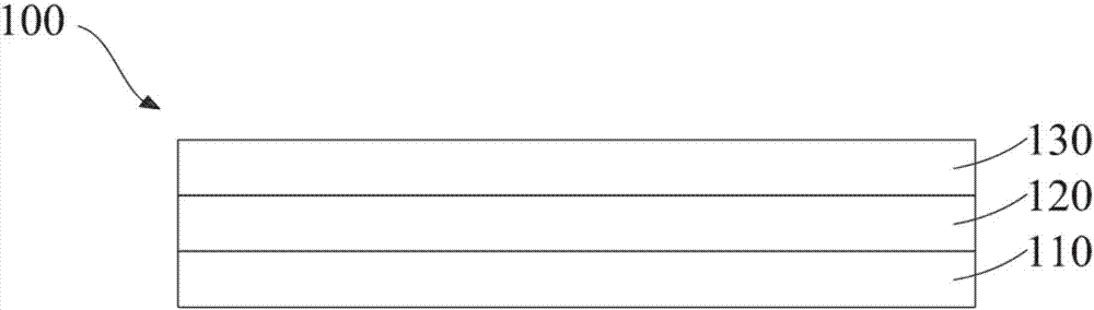
[0023] In the drawings, the thicknesses of layers and regions are exaggerated for clarity. Like reference numerals refer to like components throughout the specification and drawings.

[0024] image 3 is a schematic diagram of a packaging structure for packaging an OLED device according to an embodiment of the present invention.

[0025] refer to image 3 , according to an embodiment of the present invention, the packagin...


PUM


Abstract

The invention discloses a packaging structure for packaging an OLED device. The packaging structure comprises a packaging unit. The packaging unit comprises an optical adhesive layer; an inorganic packaging layer arranged on the optical adhesive layer; and an organic packaging layer arranged on the inorganic packaging layer. According to the invention, the optical adhesive layer is introduced intothe packaging structure. The stress strain of the inorganic packaging layer during bending is reduced, so that the cracking risk of the inorganic packaging layer is reduced. In addition, compared with the prior art, the packaging structure provided by the invention saves a barrier layer on the outermost layer of the structure. Therefore, the thickness of the packaging structure can be reduced, and the equipment thinning development can be facilitated.

Description

technical field [0001] The invention belongs to the technical field of organic light-emitting display, and in particular relates to a packaging structure for packaging OLED devices and a display device. Background technique [0002] In recent years, organic light-emitting diode (Organic Light-Emitting Diode, OLED) display device has become a very popular emerging flat-panel display device product at home and abroad, because OLED display device has self-illumination, wide viewing angle, short response time, high luminous efficiency, It has the characteristics of wide color gamut, low operating voltage, thin thickness, large-size and flexible panels and simple manufacturing process, and it also has the potential of low cost. [0003] In the manufacturing process of OLED devices, metal electrodes and organic light-emitting layers are very sensitive to water vapor and oxygen. Oxygen will oxidize the metal electrodes, and water vapor will cause oxidation and crystallization of th...

Claims


Application Information

Patent Timeline
Patent Type & Authority Applications(China)
IPC IPC(8): H01L51/52
CPCH10K50/844
Inventor 陈霞
Owner WUHAN CHINA STAR OPTOELECTRONICS SEMICON DISPLAY TECH CO LTD
Why Eureka
Try Eureka