A wide temperature and low power consumption integrated light emission component
A technology of light emitting components and low power consumption, applied in the coupling of optical waveguides, etc., can solve problems such as unsatisfactory working requirements, limited working temperature, and limited cooling efficiency, and achieve low power consumption, simple process, and high cooling and heating efficiency high effect
- Summary
- Abstract
- Description
- Claims
- Application Information
AI Technical Summary
Problems solved by technology
Method used
Image
Examples
Embodiment 1
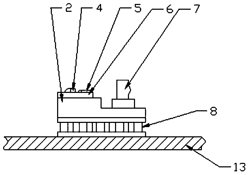
[0043] Embodiment one: if image 3 , Figure 4 , Figure 5 , Figure 6 It is a sectional view of the overall package of the optical device of the present invention. Such as image 3 , Figure 4 , Figure 5 , Figure 6 As shown, the structure of the device of the present invention includes a thermal insulation block 1, a tungsten copper heat sink 2, a thermistor 3, a backlight detector 4, a semiconductor laser chip 5, a transition block 6, a collimating optical unit 7, and a refrigerator 8 (TEC), multiplexing component 9, optical isolator 10, converging optical component 11, pin component 12, tube shell 13, tube cover 14, tube shell 13 refers to a tube shell with a high-frequency transmission line structure, and the shell can be used Cutting material, the bottom of the tube shell is made of tungsten copper, the transmission line structure is composed of multi-layer high temperature co-fired ceramics, the tube shell contains a sapphire sealed light window; the tube cover ...
Embodiment 2
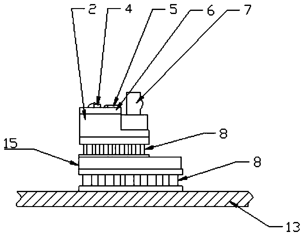
[0046] In the embodiment of the present invention, the backlight detector 4 and the semiconductor laser chip 5 are installed on the first layer cold surface 18 of the refrigerator 8 through a tungsten copper heat sink 2, and the heat emitted by the semiconductor laser chip 5 is directly pumped by the upper layer TEC onto the lower TEC.
[0047] The present invention utilizes a double-layer TEC structure to directly place the laser chip or the ALN transition block installed with the laser chip and the backlight detector on the first layer of TEC. Compared with the traditional packaging structure, the present invention has the following advantages: first, Utilizing the height difference between the first layer and the second layer of TEC, the metal tungsten copper heat sink element used for height control and heat conduction is directly removed, the components of the laser component are reduced, and the assembly process of the component is omitted, which is beneficial to improve ...
PUM
 Abstract
Description
Claims
Application Information


