Silicon substrate MOS thin film luminescent device, preparation method thereof and full-spectrum thin film luminescent device

A light-emitting device, a silicon-based technology, applied in semiconductor devices, electrical components, circuits, etc., can solve the problems of small number of conductive channels, low luminous intensity, and low luminous efficiency, and achieve improved luminous efficiency, increased number, and increased luminous intensity. big effect

Active Publication Date: 2018-05-08
XI AN JIAOTONG UNIV
View PDF5 Cites 0 Cited by
  • Summary
  • Abstract
  • Description
  • Claims
  • Application Information

AI Technical Summary

Problems solved by technology

At present, the full-spectrum thin-film light-emitting devices with existing structures have a small number of conductive channels, low luminous intensity, and low luminous efficiency.

Method used


Image

  • Silicon substrate MOS thin film luminescent device, preparation method thereof and full-spectrum thin film luminescent device
  • Silicon substrate MOS thin film luminescent device, preparation method thereof and full-spectrum thin film luminescent device
  • Silicon substrate MOS thin film luminescent device, preparation method thereof and full-spectrum thin film luminescent device

Examples


Embodiment 1

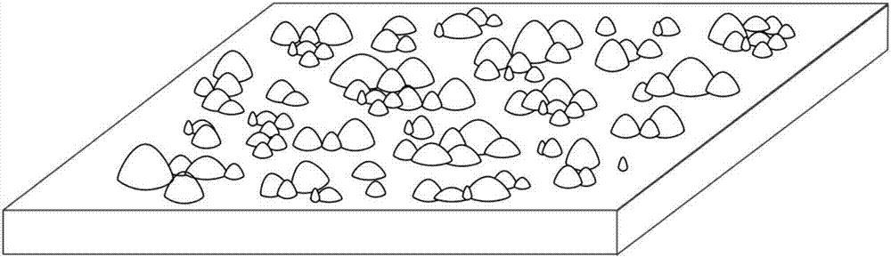
[0037] see figure 1 , a silicon-based MOS thin-film light-emitting device, using a p-type silicon wafer with a crystal orientation of as the substrate of the device, using 8% TMAH etching solution to etch the silicon substrate for 10 hours, or using 30% TMAH etching solution to etch the silicon substrate After etching for 2 hours, the etching temperature is 25°C at room temperature, and an irregular hill-shaped convex structure is prepared on the surface of the silicon substrate.

Embodiment 2

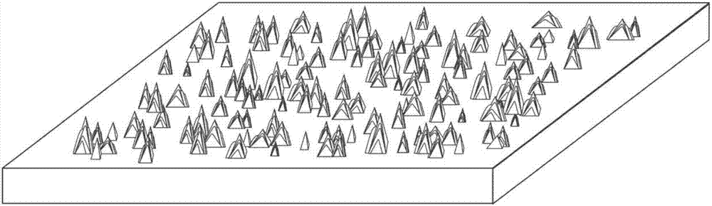
[0039] see figure 2 , a silicon-based MOS thin-film light-emitting device, using a p-type silicon wafer with a crystal orientation of as the substrate of the device, using 2% KOH solution to etch the silicon substrate for 45 minutes, and the etching temperature is 80 ° C, prepared on the surface of the silicon substrate Nested pyramid-shaped raised structures.

Embodiment 4

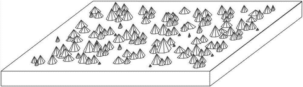
[0041] see image 3 , a silicon-based MOS thin-film light-emitting device, using a p-type silicon wafer with a crystal orientation of as the substrate of the device, using a composite solution NaOH:IPA=0.25%:6% to etch the silicon base for 15 minutes, and the etching temperature is 90 ° C. On the surface of the silicon base, a Pozierian pyramid-shaped convex structure is prepared.


PUM

PropertyMeasurementUnit
heightaaaaaaaaaa
heightaaaaaaaaaa
sizeaaaaaaaaaa

Abstract

The invention discloses a silicon substrate MOS thin film luminescent device, a preparation method thereof and a full-spectrum thin film luminescent device, and belongs to the field of thin film luminescent devices. The silicon substrate MOS thin film luminescent device comprises a silicon substrate and a bulge structure arranged on the surface of the silicon substrate, wherein the bulge structureis in the shape of one or more of a triangular prism, an irregular mountain, a nested pyramid, a pyramid like a Chinese character ''mi'', a quadranglular pyramid and a rectangular pyramid pyramid; and the distribution density on the surface of the silicon substrate, bottom size and height of the bulge structure are adjustable. Bulges of different morphologies, densities, bottom sizes and / or heights are prepared on the surface of the silicon substrate by using an anisotropic alkaline solution wet corrosion method. By using the silicon substrate with the bulge structure, the luminescent intensity of the full-spectrum thin film luminescent device forming electric channel luminescence based on MOS structure breakdown is improved, and the luminescent efficiency of the device is improved.

Description

technical field [0001] The invention belongs to the field of thin-film light-emitting devices, and in particular relates to a silicon-based MOS thin-film light-emitting device, a preparation method thereof, and a full-spectrum thin-film light-emitting device. Background technique [0002] Both traditional light-emitting diodes (LED, Light Emitting Diode) and organic light-emitting diodes (OLED, Organic Light Emitting Diode) are difficult to emit white light directly. Although there are many kinds of materials that can be used for light-emitting in the market, the light-emitting devices and light-emitting principles are also different. , but there are very few devices and materials that can directly emit excellent white light without ultraviolet and blue light excitation or three-primary color mixing, and the conventional LED and OLED white light generation methods have high costs and cumbersome preparation processes. , Integrated Circuit) process is not compatible, will caus...

Claims


Application Information

Patent Timeline
Patent Type & Authority Applications(China)
IPC IPC(8): H01L33/20H01L33/00
CPCH01L33/005H01L33/20
Inventor 张小宁林媛媛王耀功刘凌光
Owner XI AN JIAOTONG UNIV
Why Eureka
Try Eureka