Method for manufacturing ultra-diffraction limited nanometer graphics

A technology with ultra-diffraction limit and nano-patterns, which is applied in the photoengraving process, nanotechnology, nanotechnology and other directions of the pattern surface, which can solve the problem that the size of lithography cannot be further reduced, and achieve the effect of reducing the size.

Active Publication Date: 2018-05-15
张子旸
View PDF7 Cites 5 Cited by
  • Summary
  • Abstract
  • Description
  • Claims
  • Application Information

AI Technical Summary

Problems solved by technology

[0005] In order to solve the above-mentioned problems in the prior art, the present invention provides a method for preparing super-diffraction na

Method used


Image

  • Method for manufacturing ultra-diffraction limited nanometer graphics
  • Method for manufacturing ultra-diffraction limited nanometer graphics
  • Method for manufacturing ultra-diffraction limited nanometer graphics

Examples


Embodiment Construction

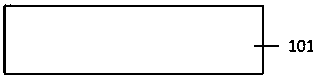
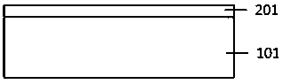
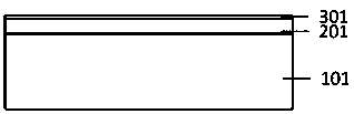
[0027] Hereinafter, embodiments of the present invention will be described in detail with reference to the accompanying drawings. This invention may, however, be embodied in many different forms and should not be construed as limited to the specific embodiments set forth herein. Rather, the embodiments are provided to explain the principles of the invention and its practical application, thereby enabling others skilled in the art to understand the invention for various embodiments and with various modifications as are suited to particular intended uses. In the drawings, the shapes and dimensions of elements may be exaggerated for clarity, and the same reference numerals will be used throughout to designate the same or like elements.

[0028] It will be understood that, although the terms "first", "second", etc. may be used herein to describe various elements, these elements should not be limited by these terms. These terms are only used to distinguish one element from another...


PUM

PropertyMeasurementUnit
Thicknessaaaaaaaaaa

Abstract

The invention discloses a method for manufacturing ultra-diffraction limited nanometer graphics. The method includes: growing a double-layer phase transition material on a substrate; selecting properstepping on a double-layer phase transition material film for laser direct writing; moving the above steps 1) and 2) on a sample to perform laser direct writing once more; removing the upper phase transition material; performing positive adhesive development or negative adhesive development to obtain the ultra-diffraction limited nanometer graphics. According to the method, a mutation in a phase transition region between the upper layer and the lower layer is caused by the aid of threshold differences of the upper phase transition material and the lower phase transition material, the volume oflower phase transition is reduced, the ultra-diffraction limited nanometer graphics are favorably manufactured by the aid of the mutation, nonlinear absorption property of the material on high-energylaser enables laser energy acting on the lower phase transition material to be more concentrated in distribution, and the graphics are therefore reduced in size.

Description

technical field [0001] The invention relates to the technical field of nano-lithography, in particular to a method for preparing super-diffraction-limited nano-patterns on a substrate by a laser direct writing device. Background technique [0002] Nanolithography is a very important step in micro-nano processing. It uses photochemical reactions to transfer circuit patterns to substrates (such as gallium arsenide substrates, silicon substrates). Since light has a submicron wavelength, optical lithography can achieve micron-scale precision micro-nano structure processing. [0003] Photolithography is becoming more and more complex as nanofabrication processes become more demanding and feature sizes of integrated circuits become smaller. Due to the existence of the optical diffraction limit (λ / 2NA, where NA is the numerical aperture), the feature size of lithography is therefore limited and it is difficult to continue to reduce. Reducing the exposure wavelength of lithography...

Claims


Application Information

Patent Timeline
IPC IPC(8): G03F7/20B82Y30/00B82Y40/00
CPCB82Y30/00B82Y40/00G03F7/2022
Inventor 张子旸王旭王美芳刘永刚
Owner 张子旸
Why Eureka
Try Eureka