Formation method of semiconductor structure

A semiconductor, hydrogen gas technology, applied in the fields of semiconductor devices, semiconductor/solid-state device manufacturing, electrical components, etc., can solve the problem that the electrical performance of semiconductor devices needs to be improved

Active Publication Date: 2018-05-25
SEMICON MFG INT (SHANGHAI) CORP +1
View PDF6 Cites 0 Cited by
  • Summary
  • Abstract
  • Description
  • Claims
  • Application Information

AI Technical Summary

Problems solved by technology

[0004] Although the introduction of high-k metal gates can improve the electrical performance of semiconductor devices to

Method used


Image

  • Formation method of semiconductor structure
  • Formation method of semiconductor structure
  • Formation method of semiconductor structure

Examples


Embodiment Construction

[0027] It can be seen from the background art that, with the continuous reduction of semiconductor device technology nodes, high-k gate dielectric materials are currently used instead of traditional silicon dioxide gate dielectric materials to improve semiconductor device leakage current and equivalent gate oxide thickness (EOT). However, the electrical performance of semiconductor devices still needs to be improved. Combined with a method of forming a semiconductor structure, the reason is analyzed.

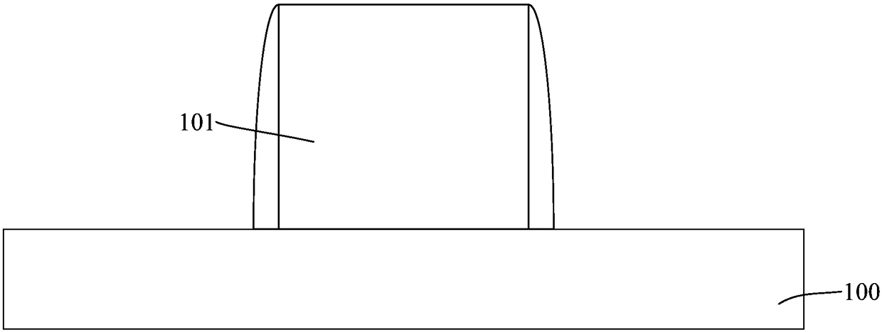
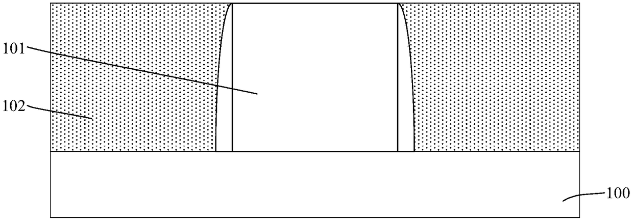
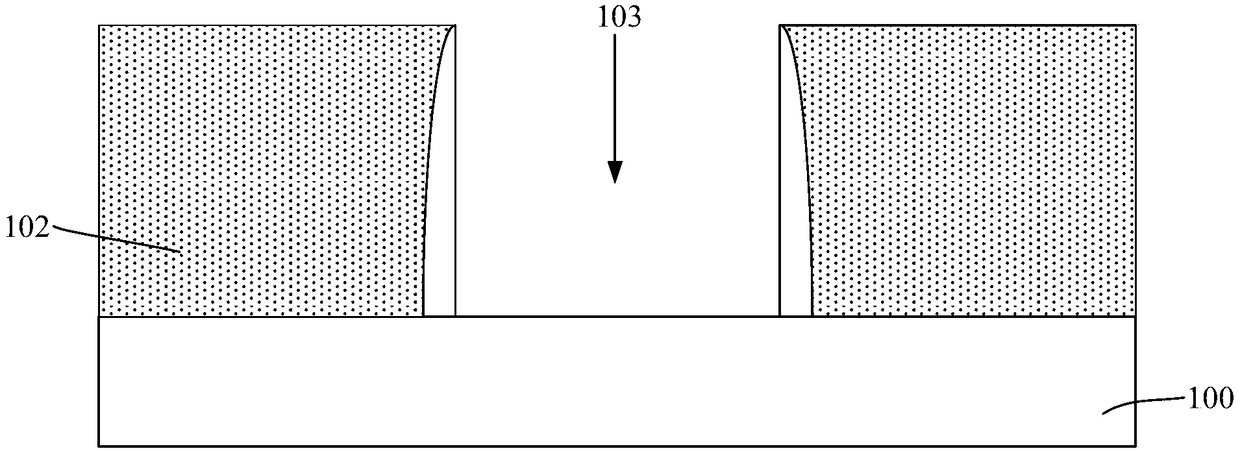
[0028] The forming method includes: providing a substrate; forming an interface layer on the substrate; forming a high-k gate dielectric layer on the interface layer by using an atomic layer deposition process; forming a gate electrode layer on the high-k gate dielectric layer .

[0029] HfO 2 It is a high-k gate dielectric material widely used at present; the corresponding precursor used in the atomic layer deposition process is mainly HfCl 4 and H 2 O. However, the formin...


PUM


Abstract

A formation method of a semiconductor structure comprises the steps of providing a substrate; forming an interface layer on the substrate; and performing a film layer formation process on the substrate for at least one time, and forming a high-k grid dielectric layer on the interface layer, wherein step of the film layer formation process comprises the steps of forming an intermediate high-k griddielectric layer on the interface layer by a chlorine-containing precursor; performing plasma processing on the intermediate high-k grid dielectric layer by employing a hydrogen-containing gas; and forming a grid electrode layer on the high-k grid dielectric layer. After forming the intermediate high-k grid electric layer and under plasmas processing, H atoms with high energy can be absorbed to Climpurity atoms in the intermediate high-k grid dielectric layer, the Cl impurity atoms deviate from a surface of the intermediate high-k grid dielectric layer, so that the content of the Cl impurityatoms in the finally-formed high-k grid dielectric layer is reduced to 0; and moreover, other impurity elements are not introduced, so that the interface performance between the high-k grid electric layer and the interface layer is improved, and the equivalent grid oxygen thickness of the high-k grid electric layer is reduced.

Description

technical field [0001] The invention relates to the field of semiconductors, in particular to a method for forming a semiconductor structure. Background technique [0002] The main semiconductor device of an integrated circuit, especially a very large scale integrated circuit, is a metal-oxide-semiconductor field effect transistor (MOS transistor). With the continuous development of integrated circuit manufacturing technology, the technology nodes of semiconductor devices continue to decrease, and the geometric dimensions of semiconductor devices follow Moore's law. When the size of semiconductor devices is reduced to a certain extent, various secondary effects caused by the physical limits of semiconductor devices appear one after another, and it becomes more and more difficult to scale down the feature size of semiconductor devices. Among them, in the field of semiconductor manufacturing, the most challenging thing is how to solve the problem of large leakage current of s...

Claims


Application Information

Patent Timeline
IPC IPC(8): H01L21/28H01L21/02
CPCH01L21/0234H01L29/401H01L29/42364
Inventor 徐建华刘海龙
Owner SEMICON MFG INT (SHANGHAI) CORP
Why Eureka
Try Eureka