Method for depositing gate dielectric, method for preparing MIS capacitor and MIS capacitor

A gate dielectric and gate dielectric layer technology, applied in the field of MIS capacitors, can solve the problems of deterioration of electrical characteristics and increase of equivalent gate oxide thickness, and achieve the effect of improving electrical performance and reducing thickness

Inactive Publication Date: 2011-10-26
SHANGHAI INST OF MICROSYSTEM & INFORMATION TECH CHINESE ACAD OF SCI
View PDF1 Cites 9 Cited by
  • Summary
  • Abstract
  • Description
  • Claims
  • Application Information

AI Technical Summary

Problems solved by technology

However, existing HfO grown by conventional ALD or PEALD 2 thin film, there is inevitably a layer of SiO with low dielectric constant between it and the substrate 2 layer, and the layer SiO 2 will grow further during annealing
In addition, HfO 2 There are usually a large number of oxygen vacancies in the film, these factors will lead to an increase in the equivalent gate oxide thickness (EOT) and deterioration of electrical properties

Method used


Image

  • Method for depositing gate dielectric, method for preparing MIS capacitor and MIS capacitor
  • Method for depositing gate dielectric, method for preparing MIS capacitor and MIS capacitor
  • Method for depositing gate dielectric, method for preparing MIS capacitor and MIS capacitor

Examples


Embodiment Construction

[0013] The present invention will be described in detail below in conjunction with the accompanying drawings.

[0014] The method for plasma-enhanced atomic layer deposition gate dielectric of the present invention comprises the following steps:

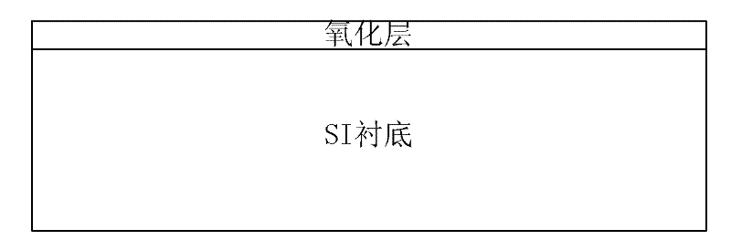
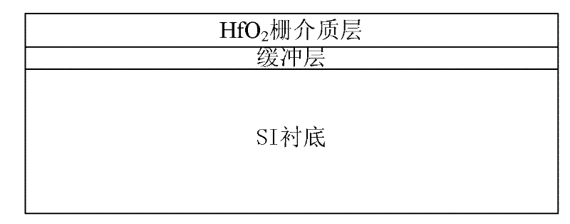
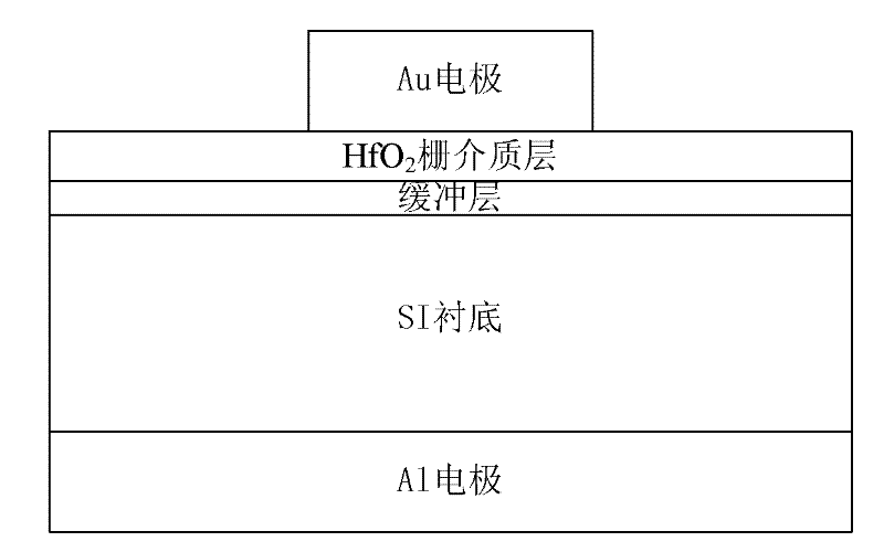
[0015] First, a semiconductor substrate is cleaned. For example, put a cut Si substrate into (NH 4 OH:H 2 o 2 :H 2 O=2:1:7) ultrasonic cleaning for 15 minutes in order to remove metal contamination on the surface of the Si substrate, followed by rinsing with deionized water, and then putting the Si substrate into a dilute HF solution (HF:H 2 (0=1:50) for about 3 minutes to remove the oxide on the surface of the Si substrate, then clean the surface of the Si substrate with deionized water, and finally dehydrate with alcohol, thereby completing the cleaning of the Si substrate.

[0016] Next, the cleaned semiconductor substrate was treated with O 2 The plasma and the nitrogen-containing plasma pretreat the surface of the semicond...


PUM

PropertyMeasurementUnit
thicknessaaaaaaaaaa
thicknessaaaaaaaaaa

Abstract

The invention provides a method for depositing a gate dielectric, a method for preparing a MIS capacitor and a MIS capacitor. The method for depositing the gate dielectric comprises the following steps: first, pretreating the surface of a semiconductor substrate by using O2 plasma and plasma containing nitrogen so as to form a nitrogenous oxide layer on the surface of the semiconductor substrate; and then, growing a gate dielectric layer with high dielectric constant on the surface of the nitrogenous oxide layer using a plasma enhanced atomic layer deposition process, wherein, the oxide layer converts into a buffer layer with higher dielectric constant than SiO2 in the process of growth of the gate dielectric layer. Based on the method for depositing the gate dielectric, a MIS capacitor is prepared by forming a metal electrode on the upper and lower surface of the formed semiconductor structure. The invention has the advantages that: the existence of the buffer layer is capable of improving the interface characteristic between the semiconductor material and the high K gate dielectric layer, reducing the increasement of equivalent oxide thickness (EOT) and improving the electric properties.

Description

technical field [0001] The invention relates to the field of semiconductors, in particular to a method for depositing a gate dielectric, a method for preparing an MIS capacitor and the MIS capacitor. Background technique [0002] With the rapid development of microelectronics technology, SiO 2 The thickness of the gate dielectric layer is getting thinner and thinner, when the SiO 2 When the thickness of the gate oxide layer is less than 1nm, the leakage current caused by direct tunneling will be so large that the device will fail. Moreover, ultra-thin SiO 2 The gate dielectric layer is also limited in terms of long-term reliability, boron penetration, and uniformity. At present, one of the effective methods to overcome these limitations is to adopt new insulating dielectric materials with high dielectric constant (high-k materials). After the high-k material is used, the physical thickness of the gate dielectric layer can be increased under the condition of ensuring the s...

Claims


Application Information

Patent Timeline
Patent Type & Authority Applications(China)
IPC IPC(8): C23C16/44C23C16/40H01L21/285H01L21/334H01L29/94
CPCH01L21/28167H01L21/28194H01L29/513H01L29/517H01L29/66181H01L29/94
Inventor 程新红徐大伟王中健夏超何大伟宋朝瑞俞跃辉
Owner SHANGHAI INST OF MICROSYSTEM & INFORMATION TECH CHINESE ACAD OF SCI
Why Eureka
Try Eureka