GaN-based HEMT device and preparation method thereof

A technology of devices and barrier layers, which is applied in the field of GaN-based HEMT devices and its preparation, can solve problems such as limiting the industrialization and application of GaN-based HEMT devices, and large losses, so as to increase the turn-on voltage, improve consistency, and improve breakdown The effect of voltage

Active Publication Date: 2018-06-01
WAYTHON INTELLIGENT TECH SUZHOU CO LTD
View PDF3 Cites 13 Cited by
  • Summary
  • Abstract
  • Description
  • Claims
  • Application Information

AI Technical Summary

Problems solved by technology

The F ion implantation technology in the gate electrode region also has the disadvantage of large loss in the channel, which limits the industrialization and application of GaN-based HEMT devices

Method used


Image

  • GaN-based HEMT device and preparation method thereof
  • GaN-based HEMT device and preparation method thereof
  • GaN-based HEMT device and preparation method thereof

Examples


Embodiment Construction

[0046] The technical solution of the present invention will be further described below in conjunction with the accompanying drawings.

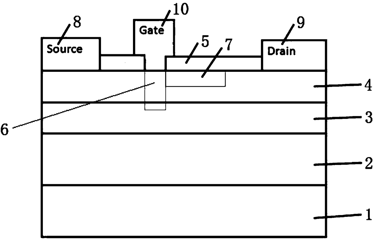
[0047] see figure 1 As shown, the above-mentioned GaN-based HEMT device includes sequentially stacked from bottom to top:

[0048] Substrate layer 1, aluminum nitride buffer layer 2, gallium nitride channel layer 3, Al(ln, Ga, Sc)N barrier layer 4, silicon nitride passivation layer 5.

[0049]The GaN-based HEMT device also includes: a P-type channel region 6 arranged in the gallium nitride channel layer 3 and the Al(ln, Ga, Sc)N barrier layer 4; The P-type diffusion region 7 in the N barrier layer 4; the source electrode 8 and the drain electrode 9 arranged on the upper surface of the Al(ln, Ga, Sc)N barrier layer 4; The gate electrode 10 on the upper surface of the barrier layer 4 is located above the P-type channel region 6 , and the gate electrode 10 is located between the source electrode 8 and the drain electrode 9 ; the P-type diffusio...


PUM

PropertyMeasurementUnit
thicknessaaaaaaaaaa
thicknessaaaaaaaaaa
thicknessaaaaaaaaaa

Abstract

The invention discloses a GaN-based HEMT device comprising a substrate layer, an aluminum nitride buffer layer, a gallium nitride channel layer, an Al(ln,Ga,Sc)N barrier layer and a silicon nitride passivation layer which are laminated from the bottom to the top in turn. The GaN-based HEMT device also comprises a P-type channel region which is arranged in the gallium nitride channel layer and theAl(ln,Ga,Sc)N barrier layer, a P-type diffusion region which is arranged in the Al(ln,Ga,Sc)N barrier layer, a source electrode and a drain electrode which are arranged on the Al(ln,Ga,Sc)N barrier layer, and a gate electrode which is arranged on the Al(ln,Ga,Sc)N barrier layer, wherein the P-type diffusion region is arranged between the gate electrode and the drain electrode. The invention also discloses a preparation method of the GaN-based HEMT device. The gallium nitride channel layer etching process involved in the manufacturing process of the GaN-based HEMT device relying on the etchingprocess in the prior art is omitted and changed into the ion injection process so that the consistency of the GaN-based HEMT device manufacturing process can be enhanced.

Description

technical field [0001] The invention relates to the technical field of semiconductors, in particular to a GaN-based HEMT device and a preparation method thereof. Background technique [0002] Wide bandgap semiconductor GaN material has become an ideal material for a new generation of semiconductor power devices due to its characteristics of large bandgap width, high critical breakdown electric field, and high electron saturation velocity. In recent years, the GaN-based HEMT device structure represented by Al(ln, Ga, Sc)N / GaN, which generates a high two-dimensional electron gas through spontaneous polarization and piezoelectric polarization, has become the mainstream GaN-based HEMT device material structure . [0003] Since the working mode of Al(ln, Ga, Sc)N / GaN devices is mostly a depletion device, in the switching circuit, the power consumption and the complexity of the design are increased. The GaN-based HEMT device can improve the safety of circuit operation, so the Ga...

Claims


Application Information

Patent Timeline
Patent Type & Authority Applications(China)
IPC IPC(8): H01L29/778H01L29/06H01L21/335
CPCH01L29/0619H01L29/66462H01L29/7786
Inventor 刘洪刚常虎东孙兵袁志鹏肖冬萍
Owner WAYTHON INTELLIGENT TECH SUZHOU CO LTD
Why Eureka
Try Eureka