Multi-die higher-order photonic switching structure based on high-density memory

A memory, high-density technology, applied in the field of high-performance computer system interconnection network, can solve problems such as the inability to meet the actual needs of high-level switching

Active Publication Date: 2018-06-01
NAT UNIV OF DEFENSE TECH
View PDF4 Cites 20 Cited by
  • Summary
  • Abstract
  • Description
  • Claims
  • Application Information

AI Technical Summary

Problems solved by technology

However, in the high-performance computing-oriented interconnection network switching chip, it is often required that the switching chip has a higher order number of 128 or even

Method used


Image

  • Multi-die higher-order photonic switching structure based on high-density memory
  • Multi-die higher-order photonic switching structure based on high-density memory
  • Multi-die higher-order photonic switching structure based on high-density memory

Examples


Embodiment Construction

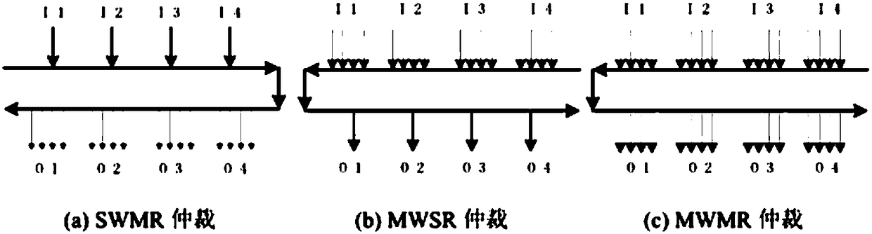
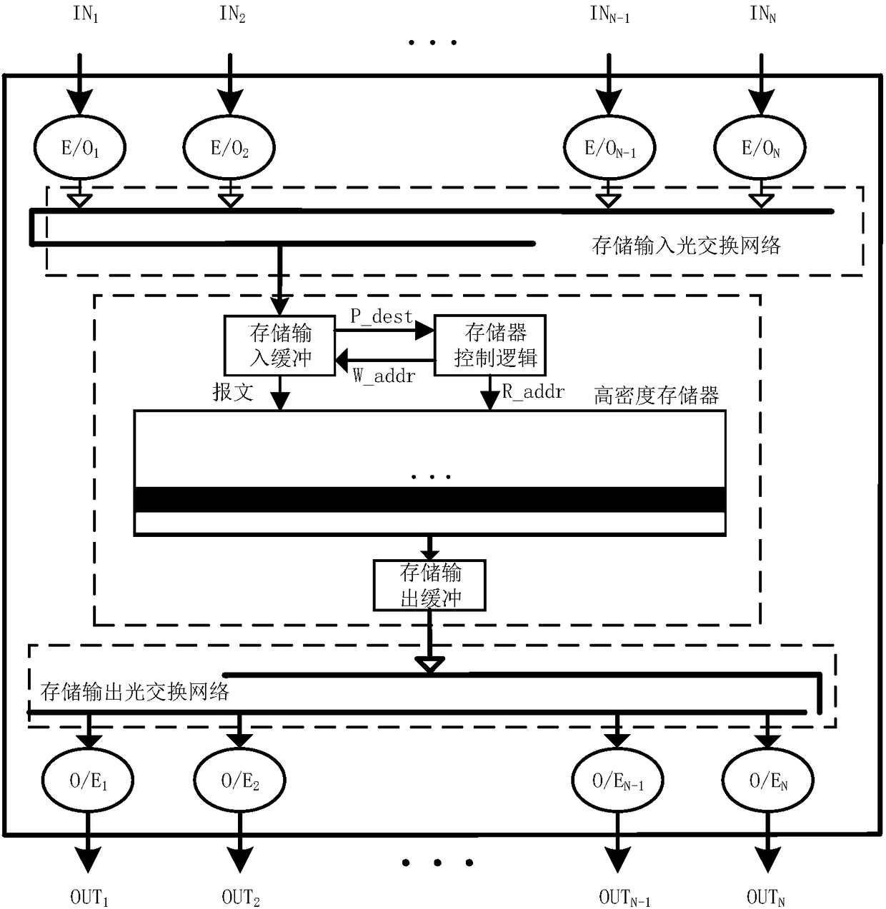
[0065]The previous analysis shows that under the condition of single-port 100Gbps, in order to prevent the high-density memory from becoming the bottleneck of the entire switching network, a single chip can support up to 40 ports to inject packets at a saturated injection rate. When designing the next-generation 64 or even When a high-end switching chip with 128 ports is used, only about 4 memory dies can be realized at most. Although the high connectivity of the fully interconnected network requires each node to provide more ports, when the network scale is small, the number of ports is completely acceptable. On the other hand, due to the point-to-point connectivity characteristics of the fully interconnected network, The number of hops for inter-chip exchange of all messages is only one step. At the same time, the fully interconnected network has features such as deadlock avoidance and livelock avoidance, which greatly simplifies the design of inter-chip routing logic. What ...


PUM


Abstract

The invention provides a multi-die higher-order photonic switching structure based on a high-density memory in order to solve the problem of limited structure of a switching chip due to the bandwidthbottleneck of the memory of the conventional photonic switching structure. The structure is formed by mutual connection of K completely same photonic switching dies based on the high-density memoriesthrough an inter-chip interconnection network and includes N input/output ports, and each photonic switching die comprises N/K input ports, N/K electro-optical conversion modules, N/K separators, a storage input photonic switching network, an optical waveguide, a storage input buffer, a memory control logic, an inter-chip interconnection input output agent module, an inter-chip input buffer, an alternative selector, the high-density memory, a storage output buffer, a storage output photonic switching network, N/K photoelectric conversion modules, and N/K output ports, wherein K, N and k are all integers, 1<=k<=K, and K<=N. According to the structure, the complexity of the switching structure and the cost of optical devices are substantially reduced, and the order of the switching structureis further extended.

Description

technical field [0001] The invention belongs to the field of high-performance computer system interconnection network, in particular to the high-order optical switching structure applied to the high-performance computer interconnection subsystem. Background technique [0002] With the running requirements of big data analysis, machine learning, large-scale commercial application optimization and other applications in High Performance Computing (HPC) systems, an interconnection network for efficient communication of distributed computing core storage resources should be constructed in HPC systems The system becomes a priority. The increase in demand for high-performance computer interconnection and communication has put forward higher requirements for the order and communication capabilities of high-end switching chips. Because high-end switching chips can reduce the network diameter while providing high bandwidth and rich routing paths, they have gradually replaced low-end ...

Claims


Application Information

Patent Timeline
IPC IPC(8): H04Q11/00
CPCH04Q11/0003H04Q11/0005H04Q11/0062H04Q2011/0007
Inventor 赖明澈翦杰肖立权庞征斌常俊胜齐星云张建民罗章董德尊徐金波黎渊
Owner NAT UNIV OF DEFENSE TECH
Why Eureka
Try Eureka