Light-emitting device and display device

A technology for light-emitting devices and electrode layers, which is applied to electric solid-state devices, semiconductor devices, organic semiconductor devices, etc., can solve the problems of reducing the performance of OLEDs, enhancing the effect of the resonant cavity, narrowing the emission spectrum, etc., so as to reduce the effect of the resonant cavity, Broad spectral emission, performance-enhancing effect

Pending Publication Date: 2018-06-05
BOE TECH GRP CO LTD
View PDF0 Cites 0 Cited by
  • Summary
  • Abstract
  • Description
  • Claims
  • Application Information

AI Technical Summary

Problems solved by technology

[0004] In the TEWOLED of the prior art, a resonant cavity is formed between the anode and the cathode. Since the cavity length of the resonant cavity formed between the anode and the cathode is short, the interference of light is enhanced, resulting in the enhancement of the resonant cavity effect, resulting in the emission of light. Narrowing of the spectrum reduces OLED performance

Method used


Image

  • Light-emitting device and display device
  • Light-emitting device and display device
  • Light-emitting device and display device

Examples


Embodiment Construction

[0021] In order for those skilled in the art to better understand the technical solution of the present invention, the light emitting device and the display device provided by the present invention will be described in detail below with reference to the accompanying drawings.

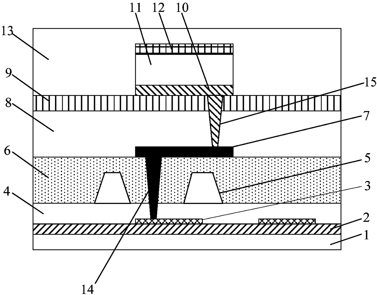
[0022] figure 1 A schematic structural diagram of a light-emitting device provided in Embodiment 1 of the present invention, such as figure 1 As shown, the light-emitting device includes a base substrate 1 and an active layer 3 disposed above the base substrate 1, a gate layer 5, a source-drain layer 7, a first electrode layer 10, an organic material layer 11 and a second electrode layer 12, the organic material layer 11 is located between the first electrode layer 10 and the second electrode layer 12, the second electrode layer 12 is located on the side of the first electrode layer 10 away from the base substrate 1, and the first electrode layer 10 is located at the source On the side of the drain lay...


PUM


Abstract

The invention provides a light-emitting device and a display device. The light-emitting device includes a substrate, and a group including an active layer, a gate layer, a source and drain layer, a first electrode layer, an organic material layer, and a second electrode layer and disposed over the substrate. The organic material layer is located between the first electrode layer and the second electrode layer. The second electrode layer is located on a side of the first electrode layer away from the substrate. The first electrode layer is located at a side of the source and drain layer away from the substrate. The first electrode layer and the source and drain layer are disposed correspondingly. The width of the source and drain layer is greater than or equal to the width of the first electrode layer. A resonant cavity is formed between the source and drain layer and the second electrode layer. The light-emitting device and the display device increase the length of the resonant cavityand weaken a resonant cavity effect, thereby achieving wide-spectrum emission and improving the performance of the light-emitting device.

Description

technical field [0001] The invention relates to the field of display technology, in particular to a light emitting device and a display device. Background technique [0002] With the rapid development of display technology, Organic Light-Emitting Diode (OLED) has made a qualitative leap in material synthesis, device preparation and process integration. OLED has many advantages such as high efficiency, high brightness, high contrast, low power consumption, fast response speed, and flexible display. It can be said that OLED will become the most powerful competitor in the next generation of mainstream flat panel display technology. Especially in the field of active matrix display, OLED has opened up a new way to realize display devices with high resolution, large area and low power consumption. [0003] In order to increase the aperture ratio of an Active-matrix Organic Light Emitting Diode (AMOLED for short), the AMOLED generally adopts a top-emitting structure. Top Emitting...

Claims


Application Information

Patent Timeline
Patent Type & Authority Applications(China)
IPC IPC(8): H01L51/52H01L51/50
CPCH10K50/80H10K50/00H10K50/856H10K59/124H10K50/828H10K50/852H10K2102/3026H10K59/805H10K59/1213H10K10/82H10K50/15H10K50/17H10K50/81H10K50/125H10K50/166H10K71/16H10K59/1201
Inventor 张粲陈小川
Owner BOE TECH GRP CO LTD
Why Eureka
Try Eureka