A three-dimensional integrated packaging of millimeter-wave antenna and silicon-based components

A millimeter-wave antenna and integrated packaging technology is applied in the field of three-dimensional integration of millimeter-wave antennas and silicon-based multi-channel components, which can solve the problems of backward packaging methods, inability to meet miniaturization and low cost, and serious microwave loss, and achieve high integration. Effect

Active Publication Date: 2020-01-03
南京国微电子有限公司
View PDF6 Cites 0 Cited by
  • Summary
  • Abstract
  • Description
  • Claims
  • Application Information

AI Technical Summary

Problems solved by technology

[0004] It can be seen from the above that the existing technology has the following problems: the RF front-end module of the antenna and components that can realize the millimeter wave operating frequency is relatively large, the microwave loss is serious, and the packaging method is backward, which cannot meet the requirements of miniaturization and low cost.

Method used


Image

  • A three-dimensional integrated packaging of millimeter-wave antenna and silicon-based components
  • A three-dimensional integrated packaging of millimeter-wave antenna and silicon-based components

Examples


Embodiment

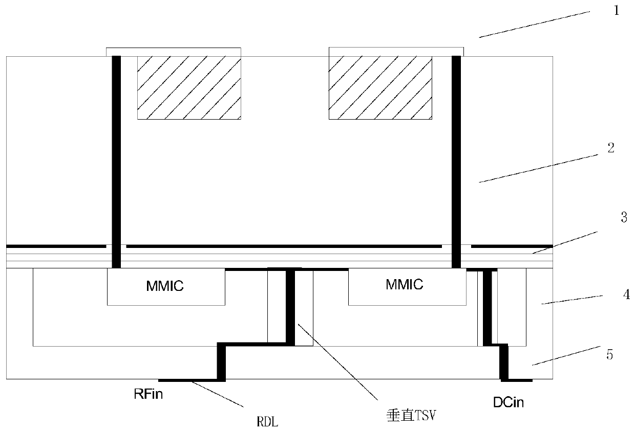
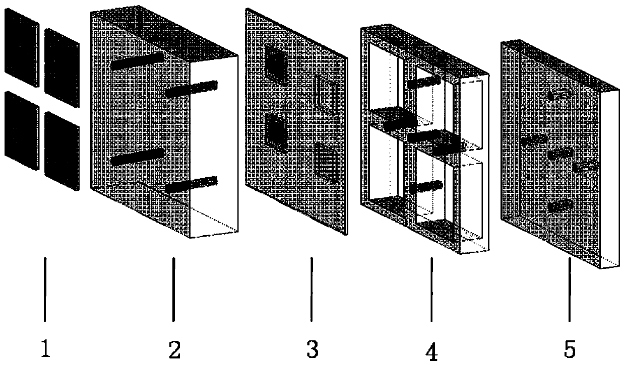
[0033] Such as figure 1 , figure 2 A three-dimensional integrated package of a novel millimeter-wave antenna and a silicon-based multi-channel component is shown. Its design architecture includes a microstrip patch antenna array, a high-resistivity silicon substrate, a BCB medium with large-scale multilayer wiring, a frame with a TSV structure, and a double-sided patterned cover.

[0034] The millimeter-wave microstrip patch antenna array is composed of 2×2 high-bandwidth, high-gain radiating elements, and its feeder is connected to the single-channel output of the component by four 3D vertically transmitted TSVs. By optimizing the three-dimensional structure and feeding network of the new radiating unit, the high gain and high bandwidth of the millimeter-wave array antenna are realized. The TSV inside the high-resistivity silicon substrate has an aspect ratio of 10:1 and is filled with metal Cu. The dielectric on the bottom surface of the high-resistivity silicon substrat...


PUM


Abstract

The invention discloses a three-dimensional integrated package based on a millimeter-wave antenna and a silicon-based multi-channel component, including a top-layer radiation microstrip patch antenna array, a high-resistivity silicon substrate with a TSV feeding structure, microwave wiring and digital The dielectric wiring layer of the wiring, the frame with the TSV three-dimensional vertical transmission structure, and the airtight packaging cover with the TSV transmission structure. The invention simultaneously integrates the microstrip patch antenna array, microwave chip, digital chip and passive device in the same module through MEMS technology, and the middle part of the surrounding frame has a TSV structure for vertical transmission of microwave signals, which has a high degree of integration and microwave Excellent performance enables multifunctionality and miniaturization of components.

Description

technical field [0001] The invention relates to a three-dimensional integration technology of a millimeter-wave antenna and a silicon-based multi-channel component, in particular to a three-dimensional integrated packaging of a millimeter-wave antenna and a silicon-based component. Background technique [0002] At present, the trend of radio frequency components is developing in the direction of miniaturization, light weight, array, and low power consumption. Traditional radio frequency components adopt LTCC + micro-assembly process, PCB board process + micro-assembly process, and the chips are interconnected through gold wire planes, and are packaged in a hermetic package. With the rise of MEMS technology, the design idea of ​​radio frequency components began to consider the use of Si substrates instead of traditional microwave dielectric ceramic substrates and PCB boards. Small loss and short delay. [0003] The traditional integration of antennas and components adopts m...

Claims


Application Information

Patent Timeline
Patent Type & Authority Patents(China)
IPC IPC(8): H01L23/58H01L23/522H01Q1/22
CPCH01L23/522H01L23/58H01Q1/2283
Inventor 沈国策周骏
Owner 南京国微电子有限公司
Why Eureka
Try Eureka