Approximate-junction microflow embedded high-efficient GaN transistor and manufacturing method thereof

A transistor and gallium nitride technology, applied in electrical solid state devices, semiconductor devices, semiconductor/solid state device components, etc., can solve the problems of device performance and reliability degradation, limiting gallium nitride device performance, and device junction temperature rise. , to achieve the effect of increasing the maximum output power, improving the efficient heat dissipation and high reliability

Active Publication Date: 2018-06-22
NO 55 INST CHINA ELECTRONIC SCI & TECHNOLOGYGROUP CO LTD
View PDF7 Cites 10 Cited by
  • Summary
  • Abstract
  • Description
  • Claims
  • Application Information

AI Technical Summary

Problems solved by technology

This is mainly because high-power microwave devices will generate a large amount of heat accumulation while outputting high power, especially for microwave power devices with an output power of hundreds of watts or even thousands of watts, which will cause a sharp rise in the junction temperature of the device and cause its device Severe degradation in performance and reliability
[0003] At present, gallium nitride-based power devices are mainly epitaxially grown on substrate materials such as silicon carbide and sapphire, and these substrate materials have low

Method used


Image

  • Approximate-junction microflow embedded high-efficient GaN transistor and manufacturing method thereof
  • Approximate-junction microflow embedded high-efficient GaN transistor and manufacturing method thereof
  • Approximate-junction microflow embedded high-efficient GaN transistor and manufacturing method thereof

Examples


Example Embodiment

[0036] Example

[0037] A manufacturing method of a near-junction micro-flow embedded high-efficiency heat dissipation gallium nitride transistor, specifically including the following steps:

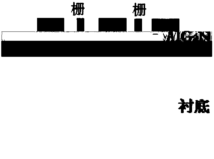
[0038] 1) Complete the conventional front-side process of a gallium nitride transistor to obtain a gallium nitride transistor, the substrate of which is SiC material, the gate-to-gate pitch of the active area is 30um, and it is a 10-gate structure;

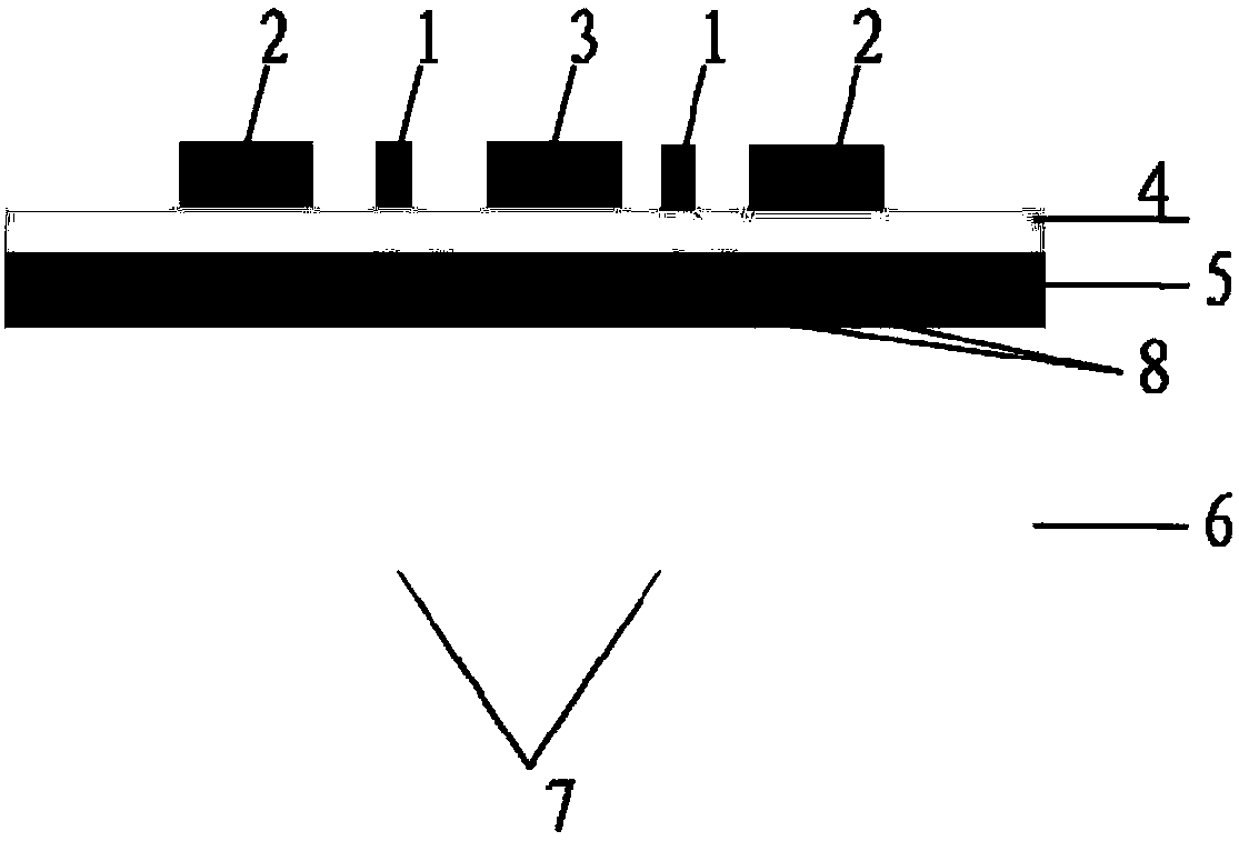
[0039] 2) Preparation of embedded micro-channels near junction area;

[0040] ①According to the size of the active area of ​​the completed gallium nitride transistor, the size of the microfluidic channel near the junction area is designed to be 20um, and its center is consistent with the center of the heat source, and its distribution is based on the active area size of 10 groups, which fully meets its heat dissipation capacity and Reliability capability.

[0041] ②Coat a silicon oxide dielectric protective layer on the front of the completed gallium...


PUM

PropertyMeasurementUnit
Widthaaaaaaaaaa

Abstract

The invention relates to an approximate-junction microflow embedded high-efficient GaN transistor and a manufacturing method thereof. The GaN transistor sequentially comprises an active region functional layer, a barrier layer, a buffer layer and a substrate layer from top to bottom, wherein the active functional layer comprises a grid, a source and a drain, and a micro fluid passage is arranged in the substrate layer and is arranged on an approximate-junction region below an active region. A fluid cooling technology is introduced into a chip, the high-efficiency cooling capability of the approximate-junction region is achieved, and the problem of heat accumulation of the active region of a large-power GaN device is solved; and compared with a traditional GaN device, the power density of the GaN transistor can be improved by 2 times or above, the maximum output power of the device is greatly improved, and relatively high reliability is maintained.

Description

technical field [0001] The invention belongs to the technical field of thermal management development of semiconductor devices, in particular to a near-junction microflow embedded gallium nitride transistor with high efficiency heat dissipation and a manufacturing method thereof. technical background [0002] The third-generation semiconductor power devices represented by gallium nitride have demonstrated their excellent high-power application characteristics. In practical applications, gallium nitride chips are based on SiC substrates, and the power density of power devices has only reached its theoretical value. One-fifth of GaN's high-power characteristics are far from being brought into play. This is mainly because high-power microwave devices will generate a large amount of heat accumulation while outputting high power, especially for microwave power devices with an output power of hundreds of watts or even thousands of watts, which will cause a sharp rise in the juncti...

Claims


Application Information

Patent Timeline
IPC IPC(8): H01L23/46H01L23/473
CPCH01L23/46H01L23/473
Inventor 郭怀新孔月婵郁鑫鑫黄宇龙吴立枢陈堂胜
Owner NO 55 INST CHINA ELECTRONIC SCI & TECHNOLOGYGROUP CO LTD
Why Eureka
Try Eureka