Electromagnetic shielding package structure having pin side wall tin climbing function and manufacturing process thereof

A technology of electromagnetic shielding and packaging structure, applied in semiconductor/solid-state device manufacturing, circuits, electrical components, etc., can solve the problems of shielding layer grounding difficulty, increase manufacturing cost and time, and save cutting cost, reduce manufacturing cost and time , The effect of improving welding performance and welding reliability

Active Publication Date: 2018-06-22
JCET GROUP CO LTD
View PDF7 Cites 0 Cited by
  • Summary
  • Abstract
  • Description
  • Claims
  • Application Information

AI Technical Summary

Problems solved by technology

[0004] However, the above-mentioned electromagnetic shielding method is more difficult to ground the shielding layer, and it needs to form additional metal posts on the substrate (see figure 1 ), electronic components, or through the TSV process to form via holes on the molding compound and fill metal fillers to form via columns. Either way, additional processes are required, which increases manufacturing costs and time

Method used


Image

  • Electromagnetic shielding package structure having pin side wall tin climbing function and manufacturing process thereof
  • Electromagnetic shielding package structure having pin side wall tin climbing function and manufacturing process thereof
  • Electromagnetic shielding package structure having pin side wall tin climbing function and manufacturing process thereof

Examples


Embodiment Construction

[0054] The present invention will be further described in detail below in conjunction with the accompanying drawings and embodiments.

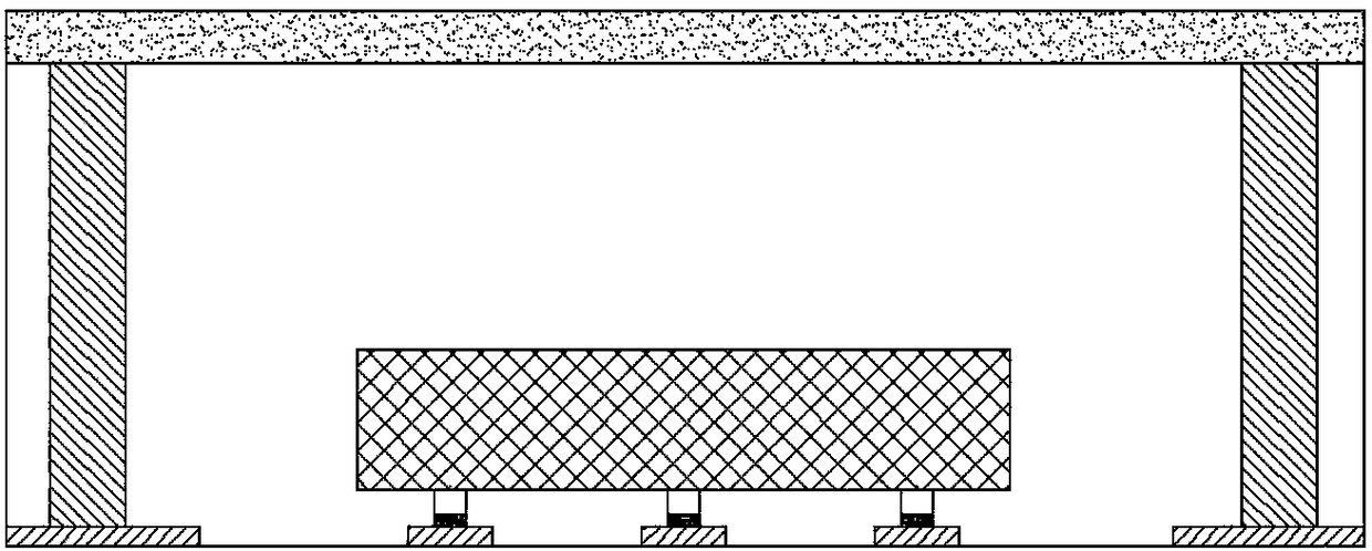
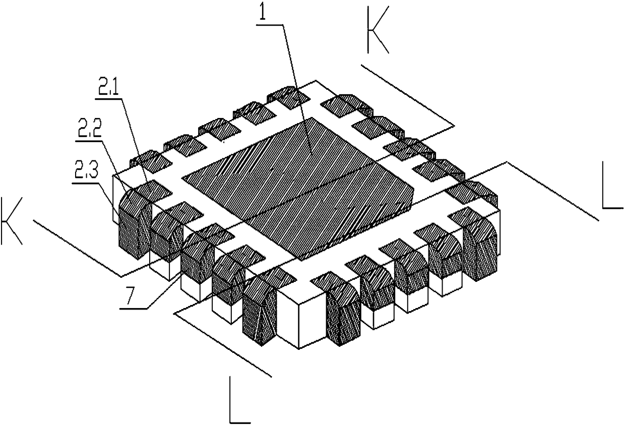
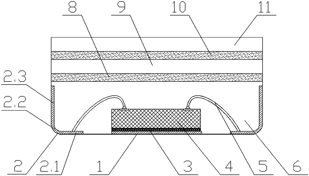
[0055] Such as Figure 2~Figure 4 As shown, in this embodiment, an electromagnetic shielding package structure with the function of tin climbing on the side wall of the pins, it includes a base island 1 and pins 2, and the base island 1 and pins 2 are metal circuit layers formed by electroplating , the pin 2 is arranged around the base island 1, the pin 2 includes a plane portion 2.1 and a side wall portion 2.3, the side wall portion 2.3 is located outside the plane portion 2.1, and the side wall portion 2.3 includes a plurality of sides The wall surface, the plane part 2.1 and the multiple side wall surfaces of the side wall part 2.3 are transitionally connected by an arc part 2.2, the convex surface of the arc part 2.2 faces the outer lower side, and the front of the base island 1 is passed through an adhesive substance Or the solder 3 is p...


PUM


Abstract

The invention relates to an electromagnetic shielding package structure having a pin side wall tin climbing function and a manufacturing process thereof. The structure comprises a paddle and pins, wherein each pin comprises a planar part and a side wall part, the side wall part comprises a plurality of side wall surfaces, the planar part and the plurality of side wall surfaces of the side wall part are in transition connection by an arc part, a chip is arranged on a front surface of the paddle, a first plastic sealing material wraps peripheral regions of the paddle, the pins and the chip, a first shielding layer is arranged on the first plastic sealing material, a second plastic sealing material is arranged on the first shielding layer, a second shielding layer is arranged on the second plastic sealing material, and a third plastic sealing material is arranged on the second shielding layer. Electroplating is performed on grooves formed by support plate etching to directly form the pins, the pins are provided with protruding arcs and the side walls, the side walls are connected with the protruding arcs, protrude out of the plastic sealing materials and have certain heights, an electromagnetic shielding layer can be directly and electrically connected with the side walls of the pins to achieve grounding, a metal post or a conductive through hole is not needed to be additionally formed, so that manufacturing cost and time are reduced.

Description

technical field [0001] The invention relates to an electromagnetic shielding packaging structure with the function of tin climbing on the side wall of pins and a manufacturing process thereof, belonging to the technical field of semiconductor packaging. Background technique [0002] As the operation speed of electronic components and the frequency of transmission signals are getting higher and higher, because integrated circuits are prone to electromagnetic interference with other internal or external electronic components, such as crosstalk, transmission loss and signal reflection, etc., the operating performance of integrated circuits subject to cuts. Therefore, the requirements of electronic components for electromagnetic interference (EMI) protection are also constantly improving. How to protect the chip in the semiconductor package from electromagnetic interference is very important. [0003] One way to reduce EMI is to shield the semiconductor package. For example, ...

Claims


Application Information

Patent Timeline
Patent Type & Authority Applications(China)
IPC IPC(8): H01L23/495H01L23/31H01L23/552H01L21/50H01L21/56
CPCH01L21/50H01L21/56H01L23/3114H01L23/49541H01L23/552H01L2224/16245H01L2224/48091H01L2224/48247H01L2224/97H01L2924/181H01L2924/00014H01L2924/00012
Inventor 王孙艳刘恺王亚琴梁志忠
Owner JCET GROUP CO LTD
Why Eureka
Try Eureka