Organic light-emitting display apparatus and preparation method thereof

A technology of light-emitting display and organic light-emitting layer, which is applied in the manufacture of semiconductor/solid-state devices, electrical components, and electrical solid-state devices, etc. It can solve the problems of easily scalding the pixel area of ​​OLED, high requirements on laser precision, and affecting production capacity. The effect of low etching cost, high etching precision and high production efficiency

Inactive Publication Date: 2018-06-26
TRULY HUIZHOU SMART DISPLAY
View PDF7 Cites 12 Cited by
  • Summary
  • Abstract
  • Description
  • Claims
  • Application Information

AI Technical Summary

Problems solved by technology

The above method requires two laser processes, which not only takes a long time and affects the production capacity, but also requires high precision of the laser, otherwise it is easy to burn the pixel area of ​​the OLED

Method used


Image

  • Organic light-emitting display apparatus and preparation method thereof
  • Organic light-emitting display apparatus and preparation method thereof
  • Organic light-emitting display apparatus and preparation method thereof

Examples


preparation example Construction

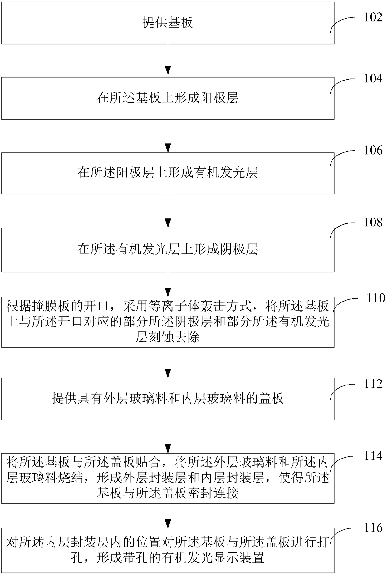
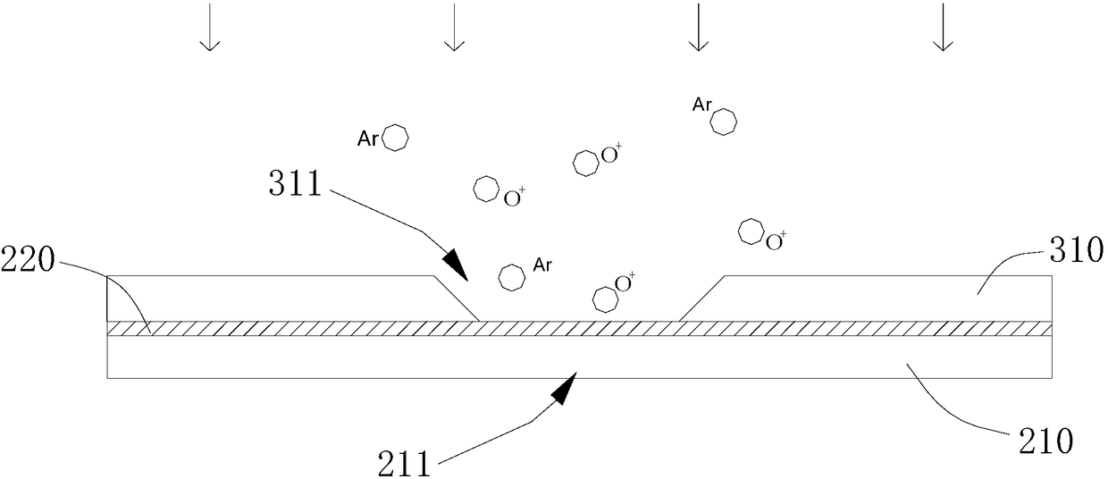
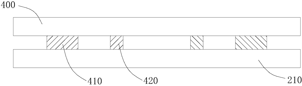
[0039] For example, a method for manufacturing an organic light-emitting display device includes: providing a substrate; forming an anode layer on the substrate; forming an organic light-emitting layer on the anode layer; forming a cathode layer on the organic light-emitting layer; For the opening of the film plate, the part of the cathode layer and the part of the organic light-emitting layer corresponding to the opening on the substrate are etched and removed by plasma bombardment; Cover plate: bonding the substrate to the cover plate, sintering the outer glass frit and the inner glass frit to form an outer encapsulation layer and an inner encapsulation layer, so that the substrate and the cover The plates are sealed and connected; the base plate and the cover plate are perforated at positions in the inner encapsulation layer to form an organic light-emitting display device with holes.

[0040] In the above embodiment, compared with traditional laser etching, the plasma bomb...


PUM


Abstract

The invention relates to an organic light-emitting display apparatus and a preparation method thereof. The preparation method comprises the steps of providing a substrate; forming a positive electrodelayer on the substrate; forming an organic light-emitting layer on the positive electrode layer; forming a negative electrode layer on the organic light-emitting layer; removing a part of the negative electrode layer and a part of the organic light-emitting layer which are corresponding to an opening in the substrate through etching by adopting a plasma bombardment mode through the opening of a mask plate; providing a cover plate with an outer layer glass material and an inner layer glass material; enabling the substrate to be laminated with the cover plate, and performing sintering on the outer layer glass material and the inner layer glass material to form an outer layer packaging layer and an inner layer packaging layer, and enabling the substrate and the cover plate to be connected ina sealing manner; and performing hole punching on the substrate and the cover plate in the inner layer packaging layer to form the organic light-emitting display apparatus with holes. By virtue of the plasma bombardment mode, more efficient organic material etching can be realized, and higher production efficiency and higher etching precision are achieved; and in addition, scalding to a pixel region can be avoided, the etching cost can be lower and the production cost can be lowered effectively.

Description

technical field [0001] The invention relates to the technical field of organic light-emitting display manufacturing, in particular to an organic light-emitting display device and a preparation method thereof. Background technique [0002] OLED (Organic Light-Emitting Diode, organic light-emitting diode) display has the advantages of self-illumination, ultra-thin, fast response, wide viewing angle, low power consumption, etc., and is considered to be the most potential display device. AMOLED (Active-matrix organic light emitting diode, active matrix organic electroluminescent device) can give full play to OLED (Organic Light-Emitting Diode, organic light-emitting diode) process is simple, high luminous efficiency, light and thin, rich colors and wide viewing angle, etc. Advantages, it can be used in large-size displays, and it can also play its potential in micro-displays. [0003] With the wide application of AMOLED, AMOLED screen needs to meet the screen design requirement...

Claims


Application Information

Patent Timeline
Patent Type & Authority Applications(China)
IPC IPC(8): H01L51/56H01L27/32
CPCH10K59/12H10K71/00
Inventor 杨帆张雪峰蔡晓义柯贤军苏君海李建华
Owner TRULY HUIZHOU SMART DISPLAY
Why Eureka
Try Eureka