
High precision N-bit dimmable delay

A technology of optical delay and delay device, which is applied in the direction of light guide, optics, instruments, etc., can solve the problems of small number of bits of delay device, large transmission loss of waveguide light, and high sensitivity of chip process, and achieves improvement of delay accuracy, The effect of improved delay step size and strong process feasibility

Pending Publication Date: 2018-06-29
SHANGHAI SILIGHT TECH
View PDF0 Cites 5 Cited by
  • Summary
  • Abstract
  • Description
  • Claims
  • Application Information

AI Technical Summary

Problems solved by technology

If submicron-scale small-sized waveguides are used, there are problems such as large waveguide optical transmission loss, low coupling efficiency between chips and optical fibers, difficulty in precise control of delay paths, and high sensitivity of chip performance to process; Large-size waveguide, the bending radius of the waveguide is relatively large, and the number of delayer bits that can be realized is small, which cannot meet the application requirements
In addition, for the multi-bit optical delayer integrated on the chip, due to the temperature dependence of the refractive index of the material, the delay variation caused by the temperature change is easily equal to or even exceeds the delay step, so the device must have a temperature control measures
In short, the current on-chip integrated "optical switch + optical waveguide delay" dimmable delay technology is still far from being practical.

Method used


Image

  • High precision N-bit dimmable delay
  • High precision N-bit dimmable delay
  • High precision N-bit dimmable delay

Examples


Embodiment Construction

[0028] The present invention will be described in detail below through specific embodiments and in conjunction with the accompanying drawings:

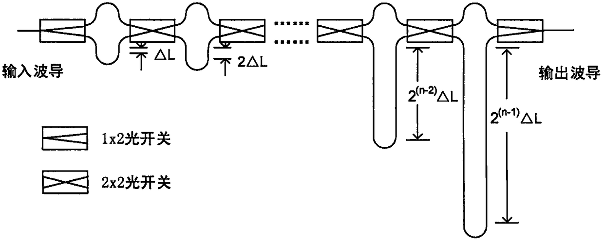
[0029] The invention proposes a novel adjustable optical delay device of "optical switch + free space optical delay", which adopts a binary topology structure. like figure 1 As shown, the optical delay unit at each level has two delay channels, and the difference between the two delay lengths is ΔL, 2ΔL, 4ΔL... 2 n-1 ΔL, where n is the bit number of the delayer, and ΔL is the tuning step size of the delayer. The 1st and N+1th optical switches in the figure can also be replaced by 2×2 optical switches.

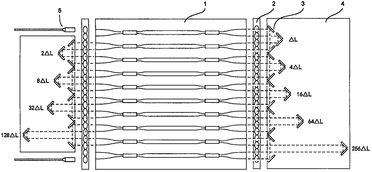
[0030] figure 2 A schematic structural diagram of an example of a 9-bit optical delay device disclosed in the present invention is given. In the figure, 1 is an optical switch chip, which consists of 10 2×2 optical switch arrays, 2 is a collimating lens array, 3 is a mirror, 4 is a mirror base platform, and 5 is an input / output fi...


PUM


Abstract

The invention provides a high precision N-bit dimmable delay. The high precision N-bit dimmable delay is mainly composed of an optical switch chip, a collimating lens array, a free space delay module,an input and output optical fiber pigtail and a pedestal. The optical switch chip is an array integration of a plurality of optical switch units. The free space delay module realizes integration of multiple levels of time delay units. High efficient coupling of the optical switch chip and the free space delay module is realized through lens array. And finally the dimmable delay having a ps levelstep length over 10-bit is realized. the invention has advantages of high delay precision, large bandwidth, small size, low weight, easy technique implementation and the like, and is suitable for light-operated phased array radar systems and especially for application in fields of onboard and space-borne radars and the like.

Description

technical field [0001] The invention relates to the technical field of optoelectronic devices, in particular to a high-precision tunable optical delay device. Background technique [0002] In the phased array radar system, the phase shifter configuration of the traditional electrical domain phased array antenna is related to the frequency of the microwave signal, which makes the instantaneous bandwidth very narrow. In order to realize the large instantaneous bandwidth of the phased array radar, the True Time Delay technology should be used to replace the electrical domain phase shifter. The traditional TTD is composed of waveguides or coaxial cables. This method of directly delaying microwave signals is limited by the density of electrical circuits. The constructed delay network is bulky and cumbersome, and has high signal loss, both in performance and engineering. Not practical. The microwave signal is modulated onto the light, and the optical waveguide is used as the del...

Claims


Application Information

Patent Timeline
Patent Type & Authority Applications(China)
IPC IPC(8): G02B6/32G02B6/35G02F1/01
CPCG02F1/01G02B6/32G02B6/3518
Inventor 李冰严亭赖龙斌
Owner SHANGHAI SILIGHT TECH
Learn More