Semiconductor device and manufacture method thereof

A manufacturing method and semiconductor technology, applied in semiconductor/solid-state device manufacturing, semiconductor devices, electric solid-state devices, etc., can solve the problems of small effect, small improvement space, and limited adjustment range of gate polysilicon film deposition temperature, etc., to achieve realization Simple and effective for improving warpage problems

Active Publication Date: 2018-06-29
SEMICON MFG INT (SHANGHAI) CORP +1
View PDF9 Cites 3 Cited by
  • Summary
  • Abstract
  • Description
  • Claims
  • Application Information

AI Technical Summary

Problems solved by technology

However, in this method, due to equipment factors, the adjustment range of the deposition temperature of the gate polysilicon film layer is limited, and there is little room for improvement, and, under the trend of increasing trench density, the role played is getting smaller and smaller.

Method used


Image

  • Semiconductor device and manufacture method thereof
  • Semiconductor device and manufacture method thereof

Examples


Embodiment 1

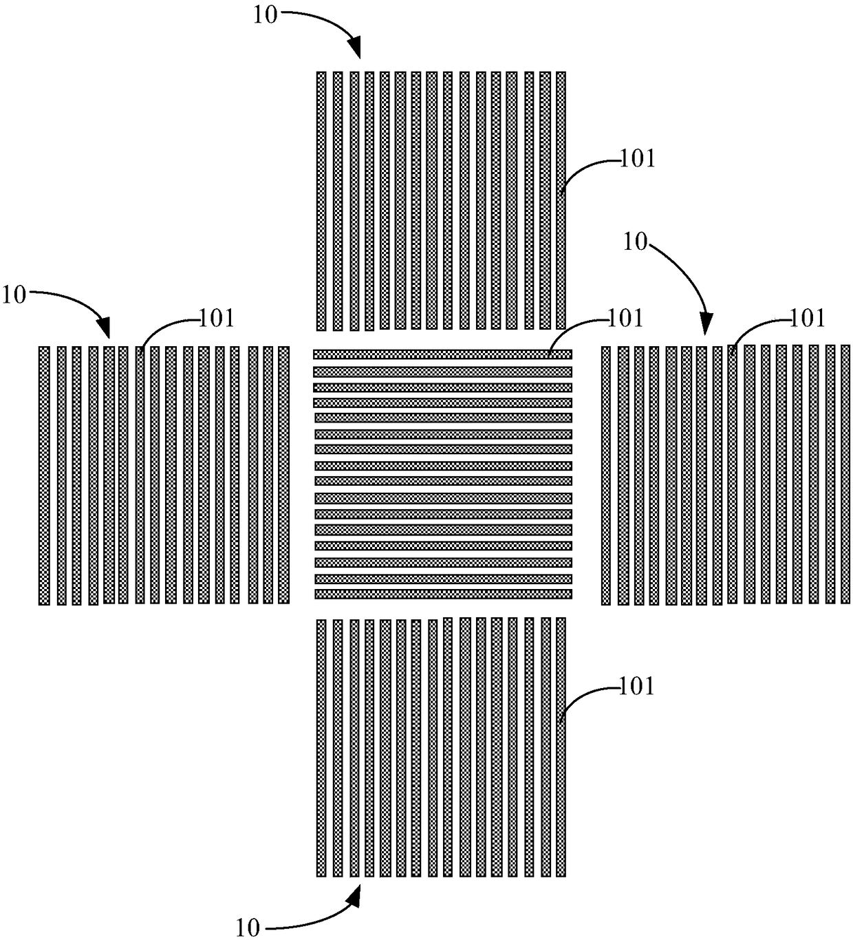
[0033] In order to improve the wafer warpage problem including multiple grooved IGBT chips, the present invention provides a semiconductor device, which mainly includes:

[0034] A wafer, on which a plurality of chips are arranged at intervals, wherein each of the chips includes a plurality of strip-shaped grooves arranged in parallel at intervals, and the strip-shaped grooves in adjacent chips are connected to each other perpendicular to each other.

[0035] The structure of the semiconductor device in the present invention keeps the strip grooves in adjacent chips perpendicular to each other, and the warpage of the wafer caused by the filling of the groove and the gate cancels each other, thereby improving the warpage problem of the whole wafer. At the same time, the conventional gate layer deposition process can also be maintained without any impact on the process, and the implementation is simple.

[0036] Below, refer to figure 1 The semiconductor device structure of th...

Embodiment 2

[0050] In order to solve the foregoing technical problems, the present invention also provides a method for manufacturing a semiconductor device, by which the structure of the semiconductor device in the foregoing implementation 1 can be realized.

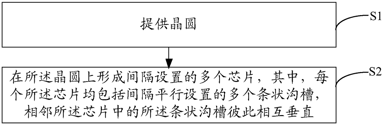
[0051] The manufacturing method of semiconductor device of the present invention mainly comprises the following steps:

[0052] Step S1, providing a wafer;

[0053] Step S2, forming a plurality of chips arranged at intervals on the wafer, wherein each of the chips includes a plurality of strip-shaped grooves arranged in parallel at intervals, and the strip-shaped grooves in the adjacent chips are perpendicular to each other.

[0054] Below, refer to figure 1 and figure 2 The method for manufacturing the semiconductor device of the present invention will be described in detail.

[0055] Specifically, step 1 is performed to provide a wafer.

[0056] The wafer includes a substrate, which may be at least one of the following mate...


PUM


Abstract

The invention provides a semiconductor device and manufacture method thereof. The semiconductor device includes a wafer. A plurality of chips are arranged on the wafer in a spaced manner. Each chip includes a plurality of strip-shaped grooves arranged in parallel and in a spaced manner. The strip-shaped grooves in the adjacent chips are perpendicular to each other. According to the invention, thestrip-shaped grooves in the adjacent chips are perpendicular to each other, wafer warping caused by groove and grid filling compensates with each other, so that the warping of the whole wafer is relieved. At the same time, a regular deposition technique for the grid layer can be kept and no influence is caused on the technique. Easy implementation is achieved.

Description

technical field [0001] The invention relates to the technical field of semiconductors, in particular to a semiconductor device and a manufacturing method thereof. Background technique [0002] Insulated gate bipolar transistor (Insu1ated Gate Bipolar Transistor, referred to as IGBT) is a common power device. The ideal IGBT has the advantages of high breakdown voltage, low conduction voltage drop, short turn-off time, and long short-circuit resistance time. . IGBT is a vertical structure device, which can be divided into planar structure and trench structure. [0003] Compared with the planar IGBT, the trench type (Trench) IGBT has obvious advantages in terms of the decrease of the saturation conduction voltage (Vcesat) and the increase of the current density. At present, it has become the mainstream design in 600V ~ 3300V IGBT products. While the trench IGBT brings advantages to the characteristics of the device, it puts forward higher requirements on the process. Wafer ...

Claims


Application Information

Patent Timeline
Patent Type & Authority Applications(China)
IPC IPC(8): H01L27/02H01L27/088H01L29/78H01L21/8234
CPCH01L21/823437H01L21/823487H01L27/0207H01L27/0886H01L29/7855
Inventor 刘剑司徒道海
Owner SEMICON MFG INT (SHANGHAI) CORP
Why Eureka
Try Eureka