Organic light emitting display device and preparation method thereof

A light-emitting display and organic technology, applied in semiconductor/solid-state device manufacturing, electrical components, electric solid-state devices, etc., can solve the problems of polluting OLED pattern areas, complicated process flow, high maintenance cost, etc., to reduce the preparation process and improve the production efficiency , the effect of reducing the preparation cost

Active Publication Date: 2018-06-29
TRULY HUIZHOU SMART DISPLAY
View PDF5 Cites 2 Cited by
  • Summary
  • Abstract
  • Description
  • Claims
  • Application Information

AI Technical Summary

Problems solved by technology

It is produced by photolithography after forming metal film by CVD, which involves PVD, Photo, etching, stripping and other processes. The process is complicated, the cost is high, and there is a certain proportion of etching residue problems.
[0007] The laser etching method is used to make the alignment mark of the package back cover, and laser equipment is required. The price of laser equipment is relatively expensive, and the maintenance cost in the later period is also high.
In addition, the principle of using the laser method to make the alignment mark of the package back cover is to etch the surface or inside of the glass. When the surface etching process is used, micro-dust will be generated. These micro-dust are extremely difficult to clean and will adhere to the cleaning line equipment. In the cleaning line equipment, it will cause cross-contamination, and even pollute the OLED patter

Method used


Image

  • Organic light emitting display device and preparation method thereof
  • Organic light emitting display device and preparation method thereof
  • Organic light emitting display device and preparation method thereof

Examples


Example Embodiment

[0035] In order to facilitate the understanding of the present invention, the present invention will be described more fully below with reference to the relevant drawings. The preferred embodiments of the present invention are shown in the drawings. However, the present invention can be implemented in many different forms and is not limited to the embodiments described herein. On the contrary, the purpose of providing these embodiments is to make the disclosure of the present invention more thorough and comprehensive.

[0036] Unless otherwise defined, all technical and scientific terms used herein have the same meaning as commonly understood by those skilled in the technical field of the present invention. The terminology used herein is only for the purpose of describing specific embodiments, and is not intended to limit the present invention. The term "and / or" as used herein includes any and all combinations of one or more related listed items.

[0037] For example, a method f...


PUM


Abstract

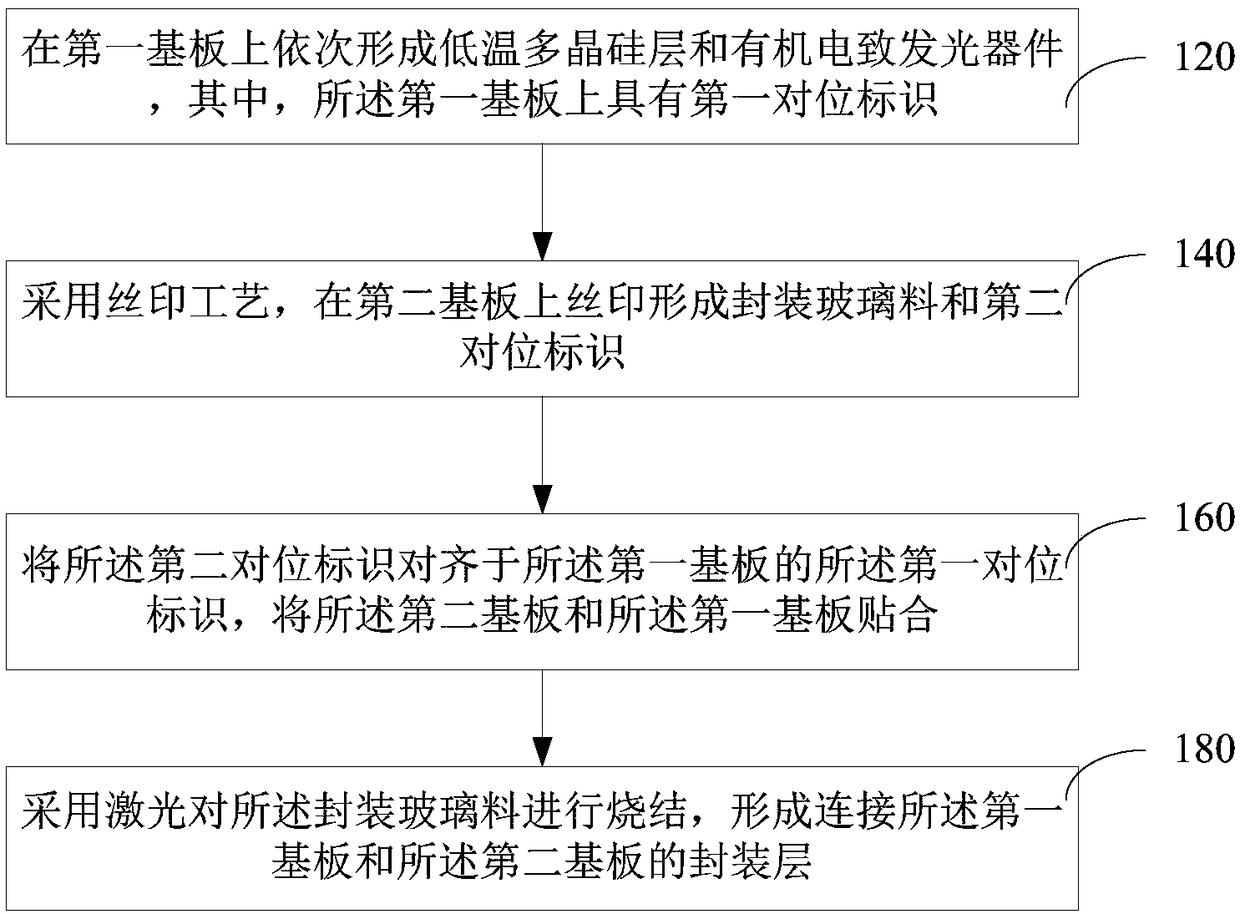
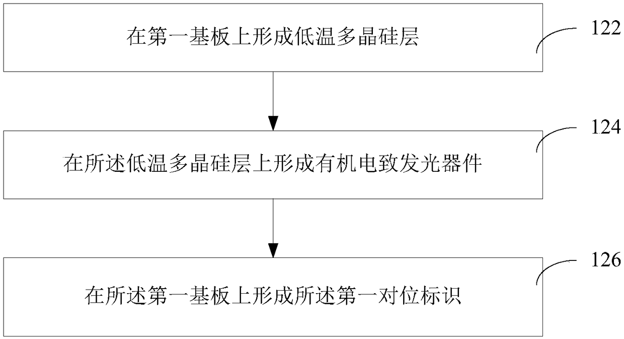
The invention relates to an organic light emitting display device and a preparation method thereof. The method comprises the following steps: a low-temperature polysilicon layer and an organic electroluminescent device are formed on a first substrate sequentially, wherein the first substrate is provided with first alignment marks; silk screen is performed on the second substrate for formation of package frit and second alignment marks; the second alignment marks are aligned with the first alignment marks of the first substrate, so that the second substrate is attached to the first substrate; the package frit is sintered by laser, and a package layer for connecting the first substrate with the second substrate is formed. The package frit and the second alignment marks are formed on the second substrate by silk screen, so that the second alignment marks are more convenient to form, the preparation process is reduced, preparation efficiency is improved, the preparation cost is effectivelyreduced, the second substrate is effectively prevented from receiving laser energy repeatedly, and breakage of the second substrate is avoided in the high-temperature process.

Description

technical field [0001] The invention relates to the technical field of organic light-emitting display manufacturing, in particular to an organic light-emitting display device and a preparation method thereof. Background technique [0002] OLED (Organic Light-Emitting Diode, Organic Light-Emitting Diode) display is considered to be the most potential display device because of its advantages such as self-illumination, ultra-thin, fast response, wide viewing angle, and low power consumption. [0003] In order to ensure the service life of the OLED device, it is usually encapsulated with an encapsulation layer to prevent oxygen and water vapor from entering the OLED device and affecting the performance of the organic light-emitting layer inside the OLED device. [0004] At present, glass powder is generally used as the packaging material for hard-screen OLED devices. Glass powder is filled in the sealing area between the rear cover and the back plate of the OLED device, and the ...

Claims


Application Information

Patent Timeline
IPC IPC(8): H01L51/52H01L51/56
CPCH10K50/841H10K50/8426H10K71/00
Inventor 宋小进汪国杰谢志生苏君海李建华
Owner TRULY HUIZHOU SMART DISPLAY
Why Eureka
Try Eureka