Ceramic/aluminum joint body, insulated circuit board, power module, LED module, and thermoelectric module
A technology for circuit substrates and ceramic substrates, applied in the direction of circuit substrate materials, circuits, printed circuits, etc., can solve the problems of insufficient joint strength and reduced joint reliability, and achieve the effect of improving joint strength and joint reliability
- Summary
- Abstract
- Description
- Claims
- Application Information
AI Technical Summary
Problems solved by technology
Method used
Image

Examples
no. 1 approach
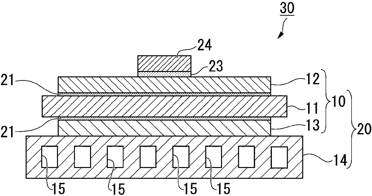
[0039] figure 1 It is a sectional view showing the ceramic-aluminum bonded body and the insulating circuit board of the first embodiment.
[0040] The ceramic-aluminum bonded body of the present embodiment is an insulated circuit including a ceramic substrate 11 as a ceramic member, a circuit layer 12 as an aluminum member bonded to an aluminum plate, and a metal layer 13 as an aluminum member bonded to an aluminum plate. Substrate 10.
[0041] Furthermore, the power module 30 of the present embodiment is formed by mounting a semiconductor element 24 such as a power semiconductor element on the circuit layer 12 of the insulating circuit board 10 via the solder layer 23 .
[0042]In addition, in the present embodiment, the cooler 14 is formed on the surface of the metal layer 13 opposite to the ceramic substrate 11 , and the insulating circuit board 20 with a cooler is provided.
[0043] The ceramic substrate (ceramic part) 11 is made of Si, which is excellent in insulation a...
no. 2 approach
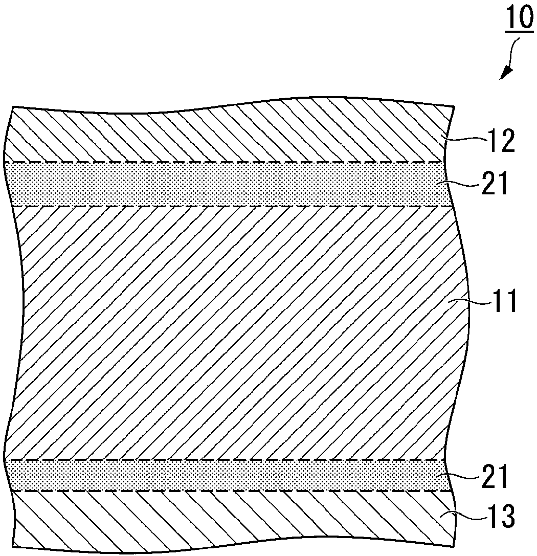
[0062] image 3 It is a cross-sectional view showing a ceramic-aluminum bonded body and an insulating circuit board according to a second embodiment.
[0063] In addition, the same code|symbol is attached|subjected to the same structure as 1st Embodiment, and the detailed description is abbreviate|omitted.
[0064] The ceramic-aluminum bonded body of the present embodiment is provided with: 3 N 4 A ceramic substrate (ceramic component) 11 made of a material containing magnesium (Mg) in (silicon nitride), provided on one side of the ceramic substrate 11 (in image 3 The circuit layer (aluminum plate, aluminum component) 12 that is the upper surface) and the other surface that is bonded to the ceramic substrate 11 (in image 3 Insulated circuit substrate (substrate for power module) 10 of metal layer (aluminum plate, aluminum member) 13 which is the lower surface).
[0065] Furthermore, the power module 30 of the present embodiment is formed by mounting a semiconductor eleme...
Embodiment 1
[0108] First, a silicon nitride substrate (40 mm×40 mm×thickness 0.32 mm) was produced by the method described in the above-mentioned embodiment so that the Mg concentration on the surface of the silicon nitride substrate became the concentration described in Table 1. In addition, the Mg concentration was determined by surface EPMA (electron probe microanalyzer) analysis. In addition, EPMA analysis was performed at 10 points (spot analysis) using FE-EPMA JXA-8530F manufactured by JEOL Ltd. under the conditions of an accelerating voltage of 15 kV and a beam current of 50 nA, and the average value thereof was regarded as the Mg concentration.
[0109] And, the Al plate ( 37mm×37mm×thickness 0.6mm), and an Al plate (37mm×37mm×thickness 1.6mm) composed of an Al plate material described in Table 1 to be a metal layer was laminated on the other surface. And, apply 5kgf / cm to them along the lamination direction 2 By heating while applying pressure, the Al plate and the ceramic subs...
PUM
| Property | Measurement | Unit |
|---|---|---|
| Thickness | aaaaa | aaaaa |
| Thickness | aaaaa | aaaaa |
| Thickness | aaaaa | aaaaa |
Abstract
Description
Claims
Application Information
 - R&D
- Intellectual Property
- Life Sciences
- Materials
- Tech Scout
- Unparalleled Data Quality
- Higher Quality Content
- 60% Fewer Hallucinations
Browse by: Latest US Patents, China's latest patents, Technical Efficacy Thesaurus, Application Domain, Technology Topic, Popular Technical Reports.
© 2025 PatSnap. All rights reserved.Legal|Privacy policy|Modern Slavery Act Transparency Statement|Sitemap|About US| Contact US: help@patsnap.com